Upcoming New 3D NAND TLC Devices: Samsung 176L & 238L, SK hynix 176L, KIOXIA/WD 162L

Dr. Jeongdong Choe
We’ve done an analysis on Micron 176L CTF CuA 3D NAND chips which was the world’s first 176L 3D NAND Flash memory device removed from Micron 3400 1TB PCIe Gen4 NVMe 1.4 cSSD.
Now, other leading 3D NAND players such as Samsung, SK hynix, KIOIXA, and Western Digital (WD) have finished the risky product stage and just moved onto the high-volume product stage with a higher yield for SSD application. The 162L/176L TLC chips have 512Gb or 1Tb memory capacity with TLC or QLC operation for UFS (mobile) or cSSD/eSSD products (ex. SK hynix Platinum P41 PCIe NVMe Gen4 SSD).
Micron revealed the 176L 3D NAND products ahead of other players last year, while other players seem to be calming their breaths in an under-supply NAND market atmosphere. Regarding the performance of the chips, it appears that all the 162L/176L 3D NAND chips look fairly competitive. For example, program throughputs are 40 ~ 50 μs and average read times (tR) are 160 ~ 184 MB/s ranges for the chips.
Again, Micron revealed a 176L CTF CuA 3D NAND chip with 195T for 512Gb TLC first. Bit density reached 10.273 Gb/mm2 for 512Gb TLC die by substantially shrinking the die size compared with the previous 128L 512Gb TLC die (7.755 Gb/mm2).
A 2-deck structure (88L+88L) has been used for the vertical NAND string integration with the other players only except Intel (3-deck structure for 144L FG CuA). For Samsung, 512Gb 176L TLC chip will be the 1st generation of Cell-on-Periphery, COP (CuA), TCAT V7 V-NAND, and the following 1Tb 238L TLC products would be the 2nd generation COP TCAT V8 V-NAND. Although the Samsung 176L TLC chip has a little lower bit density (8.5 Gb/mm2) than SK hynix 512Gb 176L V7 4D PUC NAND (10.8 Gb/mm2) and KIOXIA/WD 1Tb 162L CuA BiCS6 NAND (10.4 Gb/mm2), it’s expected to be increased to 11.5 Gb/mm2 for the Samsung 238L TLC die.
Samsung will keep the 2-deck structure even for the 238L, which is one of Samsung’s strengths in 3D NAND technology. The 162L BiCS6 3D NAND will be the 1st product with the CuA concept from KIOXIA/WD.
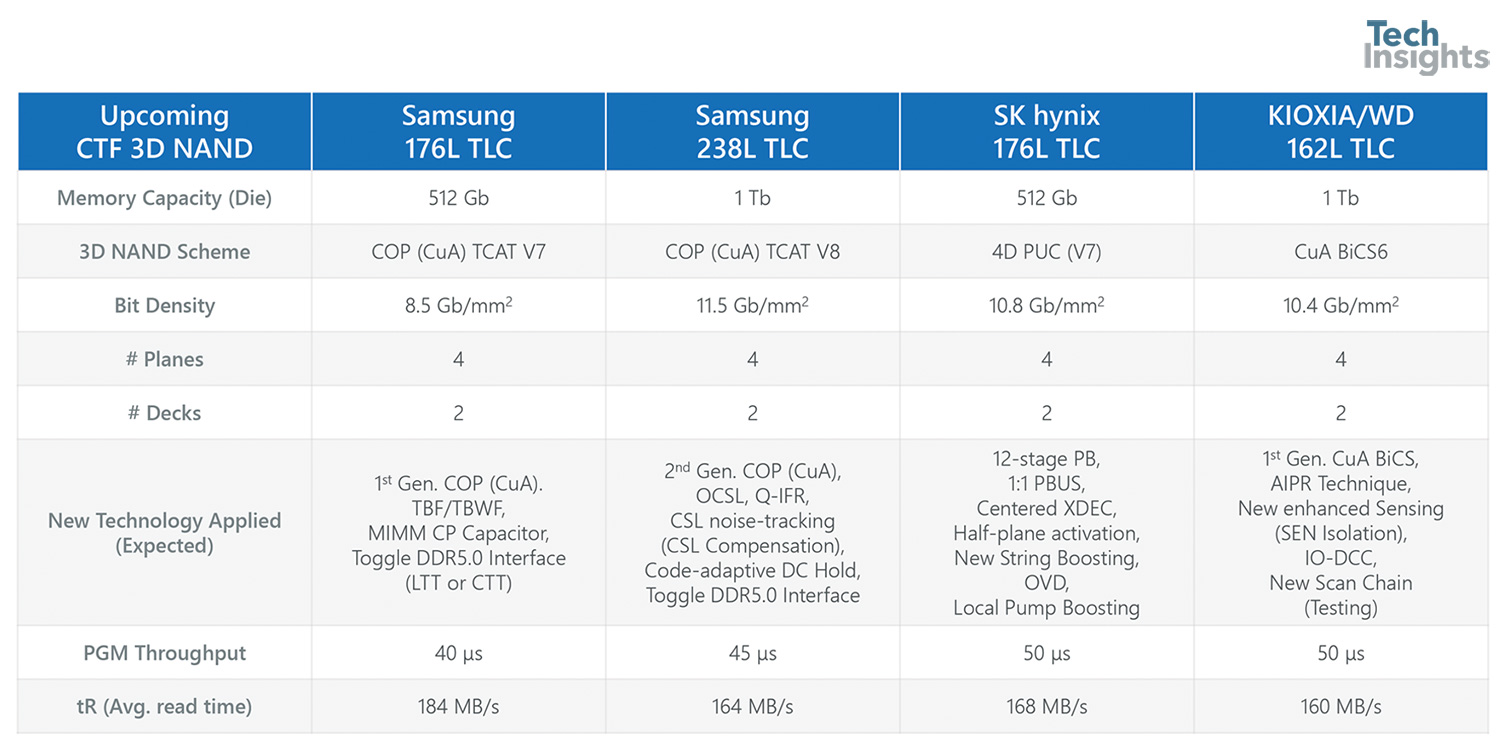
Table 1. A comparison of upcoming new 3D TLC NAND chips; Samsung 176L and 238L, SK Hynix 176L, KIOXIA/WD 162L (source: ISSCC2021, ISSCC2022)
How to increase the storage capacity of the 3D NAND in the future?
Although the industry has moved beyond 128-stacked WL structure with CuA (or PUC or COP or Xtacking) concept, the 3D NAND storage devices face a lot of challenges now such as a reduced cell string current, increased process throughput, process nonuniformity, defects, increased parasitic loads, reduced peripheral area, increased WL channel capacitance, RC delay variation, increased WL rise time and cell-to-cell interference, and decreased read/write speed.
Further, high bandwidth is also required on 3D NAND products. To achieve and overcome the challenges mentioned above, the NAND players have successfully developed and applied new innovations and technologies for upcoming 176L/238L NAND storage devices such as;
Samsung 176L TLC V7 V-NAND
- The 1st Gen. COP structure from Samsung
- 2-step BL forcing (TBF), 2-step BL/WL forcing (TBWF) to minimize cell Vt variation
- MIM vertical capacitor (charge pump, CP) to maximize the power efficiency and reduce CP area
- Toggle DDR5.0 via LTT or CTT interface
Samsung 238L TLC V8 V-NAND
- The 2nd Gen. COP structure from Samsung
- 2-deck integration
- Offset canceling sensing latch (OCSL) scheme to improve Vtrip offset
- Quad-group interference-free read (Q-IFR) scheme to reduce cell coupling (Vt shift @Read)
- CSL noise-tracking (CSL Compensation) scheme to reduce CSL noise
- Code-adaptive DC Hold to reduce tCS (set-up time) and power
- Toggle DDR5.0 Interface
SK hynix 176L TLC V7 4D PUC
- The 3rd Gen. 4D PUC NAND structure from SK hynix
- 12-stage page buffer (PB)
- 1:1 PB to cache connection bus (PBUS)
- Centered X-Decoder (XDEC) with Half-plane activation
- New String Boosting (Unselected string boosting scheme)
- Adaptive WL overdrive (OVD)
- Local pump boosting for a variable stage and frequency charge pump
KIOXIA/WD 162L TLC BiCS6
- The 1st Gen. CuA BiCS and the 6th Gen. BiCS from KIOXIA/WD
- Asynchronous independent plane read (AIPR) technique
- New enhanced Sensing (SEN Isolation) scheme
- IO duty cycle correction (IO-DCC) scheme
- New Scan Chain (Testing) for the logic circuitry

Subscribe to TechInsights Blogs
Join our list to get the latest blog posts directly in your email.


