The release of Apple’s highly anticipated A14 Bionic system on chip (SoC) followed by the M1 just weeks later in November, mark two major technology events…
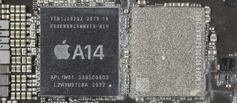
The first is that the A14 (and M1) are designed using the most advanced foundry technology available, TSMC’s N5 5nm process, and are leveraged in Apple’s new iPhone 12 and iPad Air 4.
The second is that the M1 is the first Apple Silicon to be implemented in their Mac computers and will displace Intel Core i7 CPUs in some of their products. It is this event that has the powerful M1 making headlines. The M1 chip makes Apple altogether less reliant on external sourcing for their processing components. The logic blocks used in the A14 design will almost certainly be reused in the M1 design, albeit with different core counts.
Find content like this and more in the TechInsights Platform. Sign-up for free today.
Early Architectural Changes
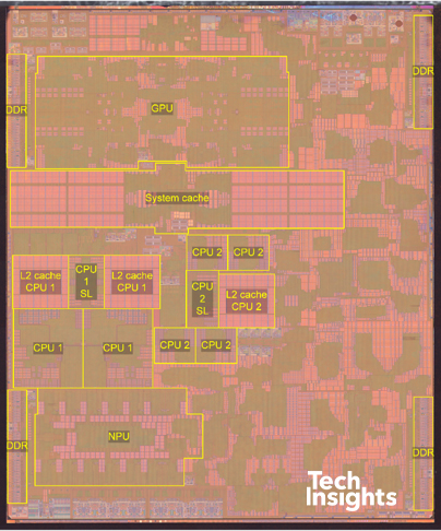
Apple's A14 Bionic SoC
Lower performance than the M1, the design is expected to be similar in nature.
Performance differences are related to the battery life for a single charge, vs. the unlimited power available to the M1 chipset.
Optimized for mobile devices with no real cooling capability and limited battery size.
This chip features a 37% smaller die size.
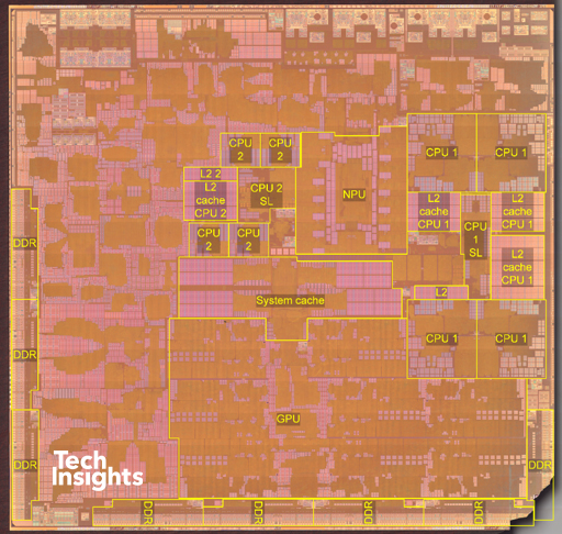
Apple's M1
SoC, not just a CPU: Contains a CPU and GPU for primary processing and graphics tasks. It also has a neural engine for AI tasks.
Larger CPU cache to speed up instruction and data access and reduce latency, but a smaller system cache.
The M1 has fewer restrictions so we see a doubling of the CPU1 and GPU cores, as well as DDR high speed memory interfaces (8 vs. 4).
Specialty blocks included, optimizing it for desktop applications where power savings is less critical. 37% die size increase of the M1 over the A14.
Die Photos and a summary table are provided below for comparative purposes.
| Change (factor) | Comments | |
|---|---|---|
| CPU 1 (mm2) | 2.1 | - |
| CPU 1 # cores | 2.0 | M1 has twice as many CPU 1 cores |
| CPU 2 (mm2) | 1.0 | Same size as CPU 2 |
| CPU 2 # cores | 1.0 | - |
| DDR (mm2) | 2.7 | M1 has double the DDR interfaces |
| # blocks | 2.0 | - |
| GPU (mm2) | 2.1 | M1 has double the GPU cores |
| GPU # cores | 2.0 | - |
| L2 cache CPU 2 (mm2) | 1.0 | ~ Same size L2 cache for CPU 2 |
| L2 cache CPU 1 (mm2) | 1.5 | M1 has a 50% larger CPU 1 L2 cache |
| NPU (mm2) | 0.9 | Same size NPU |
| System cache (mm2) | 0.8 | M1 has 25% smaller system cache |
| Total die (mm2) | 1.4 | M1 is 37% larger in die size |


