Logic Blog
A Trip Down TSMC Memory Lane
– Part 3
Dick James
February 7, 2023
At the end of Part 2 of the blog we had reached 2009 and the 40-nm generation; which put TSMC out of sync with other companies, who were marketing their 45-nm product. That discrepancy continued with the usual 70% shrink to the next node, 28-nm for TSMC and 32-nm for IDMs such as Intel and IBM.
Share This Post
Phase 5 – HKMG & Expand, Expand, Expand
In July 2010 the company announced the groundbreaking for their third 300-mm Gigafab, Fab 15, in the Central Taiwan Science Park in Taichung, to be be divided into four phases. The first phase was targeted on 40- and 28-nm technologies, with subsequent phases for the next nodes. By the end of the year Fab 12 was expanded to Phase 4 and Fab 14 to Phase 3, increasing capacity by 37% to ~2.5M 300-mm wafers/year.
In 2007 Intel introduced high-k, metal gate (HKMG) at 45-nm using gate-last, replacement metal gate (RMG) technology, using different work-function materials for NMOS and PMOS.
IBM and their associates were trying the alternative gate-first technology, which uses different capping dopants in the high-k dielectric layer to distinguish NMOS/PMOS, with a common metal and polysilicon on the high-k. This is more than just a difference in gate stack – with gate-last, all the high-temperature source/drain engineering is done before high-k deposition, using a dummy polysilicon gate; gate-first exposes the high-k layer to the high-temperature source/drain processing.
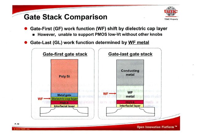
Fig.1 Gate stack comparison from 2010 Executive Forum
After starting with 32-nm R&D [1, 2], TSMC had parallel gate-first and gate-last HKMG projects for their 28-nm generation, and ultimately settled on gate-last processing, as announced at their February 2010 Executive Forum.
They also revealed that there would be three versions on offer, high-performance (28HP) and medium-speed, low-leakage varieties using HKMG (28HPL), and 28LP low-power [3] with conventional polysilicon gates, and later 28HPM for mobile (also HKMG) was added to the list [4].
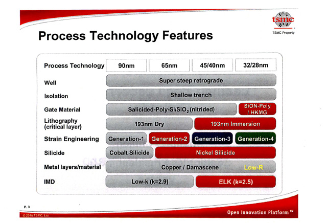
Fig.2 Process comparison from 2010 Executive Forum
Learning from the 45-nm and 40-nm delays, Restricted Design Rules were brought in to reduce variation and increase yield:
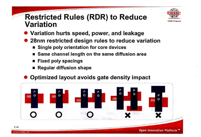
Fig.3 Restricted Design Rules for 28-nm node
As in 40-nm, 28LP continued the use of the differential oxide spacer (DOS), but this time with the use of embedded SiGe for PMOS, and no dual-stress liner.
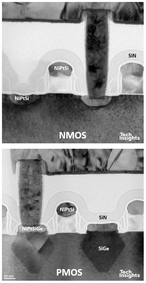
Fig.4 Cross-sections of TSMC 28LP transistors in Mediatek SoC. TechInsights, 2023.
The e-SiGe strain was enhanced by increasing Ge content to 40% and using a selective (111) cavity etch, and presumably there was some tensile stress in the contact etch-stop layer. Channel direction reverted to <110>.
Moving to the HKMG processes, Xilinx adopted 28HPL for their Kintex-7 FPGA:
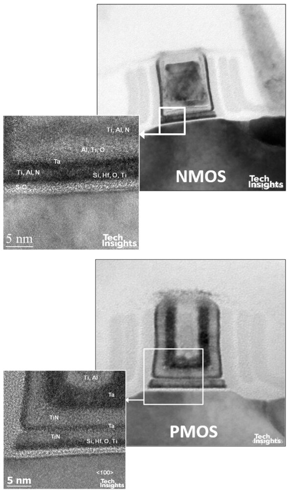
Fig.5 Cross-sections of TSMC 28HPL transistors in Xilinx Kintex 7 FPGA. TechInsights, 2023.
The high-k layer and its interfacial oxide were formed first, before the dummy polysilicon gate (high-k first), and the DOS spacer has evolved to a triple SiN/SiO/SiN spacer. In keeping with the low-power designation, there was no embedded SiGe to enhance PMOS, though we have a <100> channel orientation.
Altera chose to use 28HP for their Stratix-V product, and while the NMOS transistors look very similar, PMOS gets the benefit of e-SiGe, cranked up to ~50% Ge:
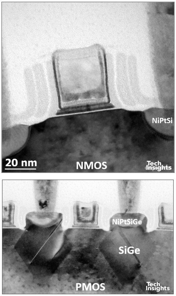
Fig.6 Cross-sections of TSMC 28HP transistors in Altera Stratix-V FPGA. TechInsights, 2023.
For reference, these are the Intel 45-nm transistors:
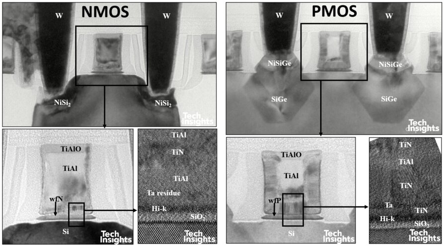
Fig. 7 Cross-sections of Intel 45-nm transistors. TechInsights, 2023.
The gate stacks are similar, but not the same, with similar work-function materials. One noticeable difference was the replacement metal sequence – Intel formed the PMOS metal stack first, the etched it back in the NMOS regions and deposited the NMOS stack; TSMC did the opposite, laying down NMOS first, etching back, and then filling in the PMOS metals.
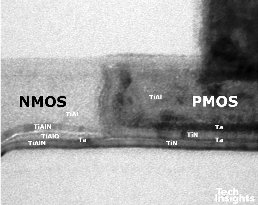
Fig.8 Linear section of TSMC 28HPM gate in Qualcomm APU. TechInsights, 2023.
To finish the sequence, 28HPM appeared to have the same gate HKMG gate stacks, but shorter minimum gate lengths (32 -> 27 nm), and the PMOS source/drain Ge content was reduced to ~30%. Both 28HP and 28HPM have <110> channel direction, in keeping with the (111)-etched SiGe cavities. All 28-nm versions seemed to utilize ELK (likely Black Diamond II) for the lower metal layers.
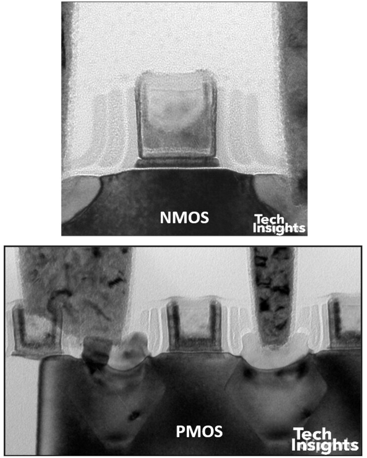
Fig.9 Cross-sections of TSMC 28HPM transistors in Qualcomm Snapdragon 800. TechInsights, 2023.
The table below summarises the processes.
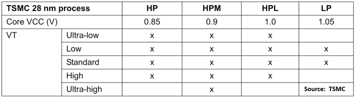
Table 1. 28-nm process variants
TSMC also announced at the 2010 Executive Forum that their next node would be 20 nm rather than 22 nm, keeping to the 70% shrink, and projected for 2012.
In the meantime Fab 15, Phase 2 started construction in mid-2011 and in December they broke ground on Phase 3; equipment move-in to Phase 1 was complete, with volume production scheduled for early 2012. By the end of 2011 Fab 12 and 14 had installed capacity of over 270,000 wafers/month, and Fab 15 was expected to add more than 100,000 to that total when complete. That was despite 2011being a challenging year, as the global semiconductor market growth was close to zero.
The 2011 Business Overview announced the development of CoWoS 3D chip stacking; “In 2011, we demonstrated a fully functional sub-system, having logic chip with built-in passive components, and bumps, all manufactured and assembled at TSMC, using our proprietary Chip on Wafer on Substrate (CoWoSTM) technology.”
CoWoS was part of a whole new train of advanced packaging development in TSMC, but that is a big enough topic that it should be covered as a separate blog.
In R&D, they also started full scale 14-nanometer finFET development, after three years of path-finding and demonstrating FinFET transistor capabilities in 28-nanometer and 20-nanometer. They also started a 450-mm program and joined the G450C (Global 450mm Consortium) in Albany, New York – which of course ultimately died.
2012 and 2013 saw the expansion of 28-nm production to where it became 22% and 34% of year-end revenue, respectively. Volume production of 20-nm product started in early 2014, and with a rapid ramp achieved 21% revenue by Q4, thanks to its use in leading smartphones, and with 28-nm made up 42% of annual revenue.
The 20-nm node required the use of double patterning for critical layers since it pushed lithography beyond its single-exposure resolution limit, with nominal Mx pitch of 64 nm [5]. It also introduced single-gate diffusion breaks and M0 local interconnect.
In terms of transistor structure, the gate stack moved to high-k last, depositing the high-k dielectric layer deposited after polysilicon removal.
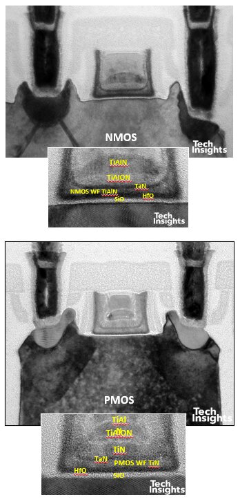
Fig.10 Cross-sections of TSMC 20HPM transistors in Qualcomm modem. TechInsights, 2023.
The replacement metal sequence reverted to the Intel style, PMOS before NMOS; and NMOS stress was enhanced by the use of stacking faults [6, 7].
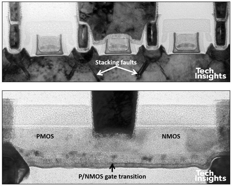
Fig.11 Cross-section of NMOS gates and source/drains (top) and linear section of gate in TSMC 20HPM transistors (bottom). TechInsights, 2023.
Stacking faults are not normally what we want to see in transistors, because they can be leaky if they go through a junction, but as long as they are contained within the source/drain diffusions, they should not be a problem.
At an intuitive level it makes sense that this mechanism should work – a stacking fault is a missing layer of atoms within the crystalline lattice, and with a ~28 nm gate length we are now working with channel lengths of a hundred atomic spacings or less. So, if a couple of atomic layers are missing at opposing ends of the channel, it seems logical that tensile stress would be induced in the channel.
We started this blog part in 2009; by 2014, TSMC’s wafer capacity had increased from ~4.4M 12” equivalent wafers/year to ~8.3M, an expansion of ~88%, funded by a total capital expenditure of ~US$ 40 billion. TSMC’s market share of the foundry business grew to 54 percent in the five years to 2014.
Mention was made earlier of 14-nm finFET R&D; somehow that morphed to 16-nm finFETs, which went into production in the third quarter of 2015.
Phase 6 – FinFETs!
To be continued…
References
[1] C.H. Diaz et al., “32nm Gate-First High-k/Metal-Gate Technology for High Performance Low Power Applications”, IEDM 2007, pp. 263 – 266
[2] S-Y. Wu et al., “A 32nm CMOS Low Power SoC Platform Technology for Foundry Applications with Functional High Density SRAM”, IEDM 2008, pp. 629 – 632
[3] S-Y. Wu et al., “A Highly Manufacturable 28nm CMOS Low Power Platform Technology with Fully Functional 64Mb SRAM Using Dual/Tripe Gate Oxide Process”, VLSI 2009, pp. 210 – 211
[4] S.H. Yang et al., “28nm Metal-gate High-K CMOS SoC Technology for High-Performance Mobile Applications”, IEDM 2011, pp. 210 – 211
[5] G. Nallapati et al., “Cost and Power/Performance Optimized 20nm SoC Technology for Advanced Mobile Devices”, VLSI 2014, pp. 156 – 157
[6] K-Y. Lim et al., “Novel Stress-Memorization-Technology (SMT) for High Electron Mobility Enhancement of Gate Last High-k/Metal Gate Devices”, IEDM 2010, pp. 229 – 232
[7] C. Weber et al., “Modeling of NMOS Performance Gains from Edge Dislocation Stress”, IEDM 2011, pp. 801 – 804


