Logic Blog
A Trip Down TSMC Memory Lane – Part 2

Dick James
To start Part 2 of the blog, we backtrack to 1998, when the 0.25-µm process was launched. One of the comments from Shang-Yi Chiang’s (former VP of R&D at TSMC) oral history was that when he joined in 1997, TSMC could not get papers accepted at conferences such as IEDM or the VLSI Symposia. However, by 1996 the foundry model was recognized, and F.C. Tseng (SVP Operations) gave a plenary talk [1] at IEDM that year. We found their 0.25-µm technology detailed at VLSI 1998 [2].
The 0.18-µm (180-nm) process was presented at VLSI 99 [3], and interestingly it spoke of the use of spin-on low-k dielectric (hydrogen silsesquioxane (HSQ)) for planarization. Shang-Yi Chiang tells the story:
“We tested it and everything was great. So we use HSQ to replace FSG (Fluorosilicate glass). It was great. … In R&D, we had to do some reliability qualification. It passed all the criteria when the production. But when you have a large volume, we began to have a reliability problem. And we found at the last moment, after we already went to production. And then it was around the Christmas time and we immediately we tried to put the FSG back, so again we worked days and at night, no break for Christmas, no break for New Year, no break for Chinese New Year. All the way and under very high pressure, and we finally get it, it’s out, and it’s already late, but good.”
So, it’s a good example of how apparent R&D success can stumble when volume manufacturing starts up. Similarly, IBM also had problems with their SiLK low-k spin-on material and had to revert to CVD processing.
Phase 3 – Drawing Level, and Even (Briefly) Ahead
Arguably with the 180-nm node, TSMC was on par with the other leading manufacturers, maybe a few months behind in dimensions but a little bit ahead with the use of FSG. IBM and Intel launched their 180-nm generations in 1998–1999, but we have no record of FSG use. They had also shipped 300-mm customer wafers in 2000 from the Fab 6 12-inch pilot line in Tainan.
The 150-nm node was essentially a shrink of 180 nm, with seven metals and FSG dielectric.
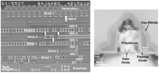
Figure 1: Cross-sections of 150-nm Nvidia GPU
The worst year in the history of the IC market was 2001, registering a decline of 32%. Despite this, 150-nm product achieved 21% of sales by Q4, and Fab 12 started 300-mm production, although overall wafer shipments were down. Surprisingly, even during the slump, 300-mm wafers achieved 4% of total silicon shipped in 2001.
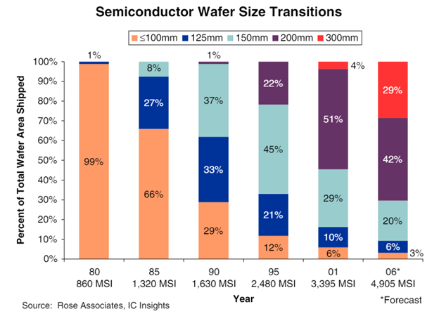
Figure 2: Semiconductor Wafer Size Transitions
The year 2002 marked the end of the lease and retirement of Fab 1 from ITRI and the volume launch of the 130-nm generation, generating 8% of sales in the fourth quarter.
RC delays in the back-end metal/dielectric stack continued to push the need for copper metallization and low-k dielectrics. IBM had introduced copper at 180 nm, and it was clear that the rest of the industry would have to follow as dimensions continued to shrink.
At 150 and 130 nm, TSMC introduced copper metallization for the first year or two, with FSG for the back-end dielectric. The stack uses single damascene copper for metal 1 with tungsten plugs (copper is a potential carrier lifetime killer if it penetrates into the substrate) and dual-damascene for the metallization above.
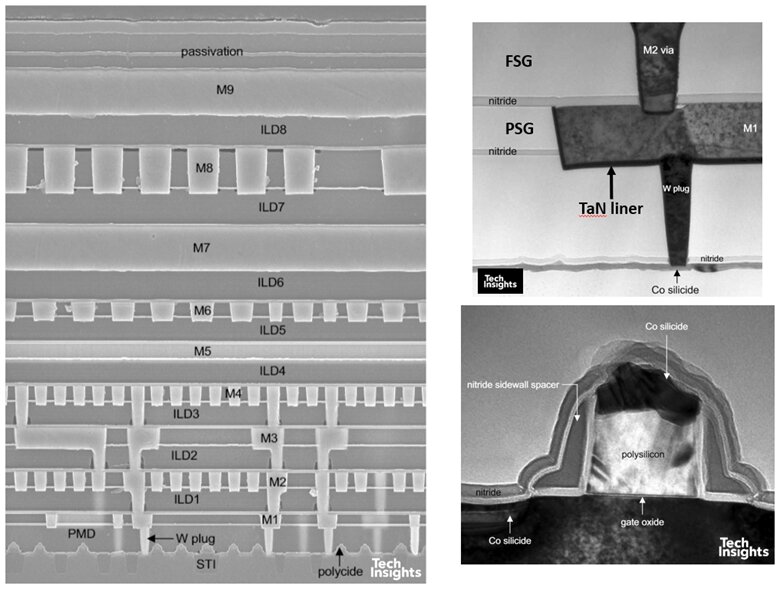
Figure 3: Cross-sections of 130-nm Altera PLD (200 mm wafer)
In April 2003, they announced the version of 130 nm with true low-k dielectrics , using Applied Materials’ Black Diamond technology. By “true low-k” we mean a dielectric with a k-value of 3.0 or less; Black Diamond was claimed to have k~2.8 [4].
Initially both were fabbed on 200-mm wafers, but having established copper, and with 300-mm ramping up, TSMC were the first company to ship product with copper and low-k dielectric in volume, some of it on 300-mm wafers. In retrospect, that put them ahead of the other foundries and IDMs such as Intel or IBM.
The first product that we saw was an ATI graphics chip, but not until the tail end of 2003.
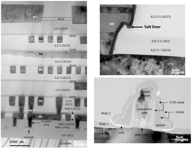
Figure 4: Cross-sections of 130-nm ATI Graphics Processor with low-k dielectric (200 mm wafer)
As usual, TSMC offered an interim 110-nm node before moving to 90 nm, typically a 10% shrink of the 130 nm, but in this example from Nvidia it looks as though it was also cost reduced, since there is no low-k in it (somewhat surprising for a GPU!). As a result, the trench and via etching are noticeably more precise than in the ATI part.
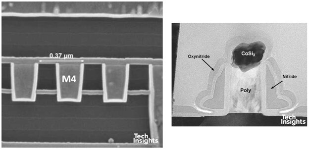
Figure 5: Cross-sections of 110-nm Nvidia Graphics Processor (300-mm wafer)
In 2004, it was the year of 90 nm, and the industry finally switched to naming its processes in nanometres rather than micrometres. It was also a seminal year for CMOS; Dennard scaling (simultaneously reducing gate length, gate oxide thickness, and drive voltage) finally reached its limit as the gate oxide became so thin (~ 1.0–1.2 nm) that carriers could tunnel through it, significantly increasing current leakage and power losses.
Having slowed down a bit at 130 nm, not using low-k , and belatedly moving to copper metal, Intel arguably took the technology lead with the introduction of strained silicon to increase carrier mobility as well as low-k . They were not unique in this, other companies also applied mobility enhancement; IBM, AMD, and Fujitsu also used tensile nitride. Fujitsu and Texas Instruments used wafer rotation, but only Intel used the embedded SiGe source/drain technique to enhance PMOS.
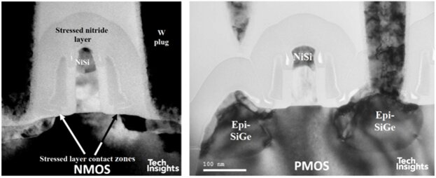
Figure 6: Intel 90-nm transistors showing stress mechanisms
Phase 4 – 300 mm, Consolidation and the Start of Domination
TSMC’s 90-nm process was its first to be produced solely on 300-mm wafers, and they claimed it was “the world’s first 12-inch, low-k, 90-nanometer process to reach full production”, and it was adopted by more than 30 customers that year.
The product analyzed by Chipworks was the Altera Stratix™-II FPGA. This is a 10-metal part (9 Cu + 1 Al), using low-k at M1–M6. The transistor structure is not a direct shrink from the 130-nm node; it has been modified to change the sidewall spacer structure from the typical L-shaped spacer of previous process generations. Compared with the Intel structure, the nitride overlayer appears to be too thin to be used as a stress layer for mobility enhancement.
The other major feature of the TSMC 90-nm process was its evolution towards a second-generation low-k dielectric process—the trench and via etching are noticeably cleaner than at the 130-nm node, and the cap layer has changed to a SiCO (rather than SiCN) composition.
Figure 7: Cross-sections of 90-nm Altera Stratix FPGA and 55-nm gate length
Ten years after going public, TSMC had two 12-inch wafer fabs, five 8-inch wafer fabs, and one 6-inch fab as well as two wholly owned subsidiaries, WaferTech in the US and TSMC (Shanghai) Company, Ltd. in China and a joint-venture fab, SSMC, in Singapore. The total installed annual capacity of TSMC and its affiliates was 4.8 million 8-inch equivalent wafers.
In the background, corporate R&D was working steadily at new transistors and process technologies such as SOI, finFETs, MRAM, high-k gate dielectrics, metal gates, strained-Si, and even nanowires. The mention of finFETs surprised us until we remembered that Chenming Hu was CTO of TSMC from 2001 to 2004 (Chenming published the first finFET paper in 1999).
They were also one of the first companies working on immersion lithography with ASML and Nikon, and they received their first ASML system in 2004, announced functional 90-nm test chips that year, and a near-production defect density of 0.014/cm2 on 12-inch wafers in early 2006.
Since the early days TSMC had offered variations on the base logic processes, such as mixed-signal, embedded memory, nonvolatile memory, and high-voltage technologies and by the mid-2000s had strategized them as two “platforms”—Advanced Technology and Mainstream Technology.
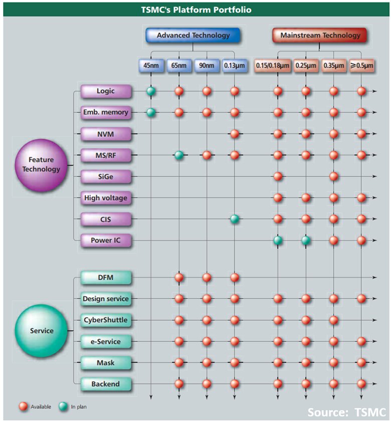
Figure 8: TSMC Platform Portfolio
We don’t have time or space to go into the details of these other “mainstream” products, but it’s worthwhile to note that 150 nm and larger, fabbed on 6-inch and 8-inch wafers, made 50% of sales in 2006.
Early 2006 saw the launch of the 80-nm half-node, as usual a lithographic shrink of the 90-nm process. These half-nodes could be difficult to identify, since they look structurally similar to the previous full node, but a detailed comparison of the metal pitches can indicate such a device.
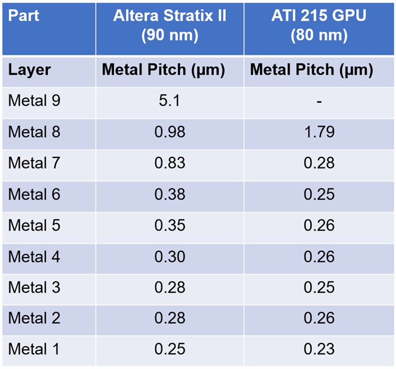
But as we can see there is little difference structurally, a subtle change to a SiOCN barrier layer, and we found a slightly larger gate length.
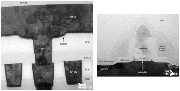
Figure 10: Cross-sections of 80-nm ATI GPU
By the end of 2006, IC Insights ranked TSMC as the fourth in IC sales, and it was the largest foundry by more than 2.5 times.
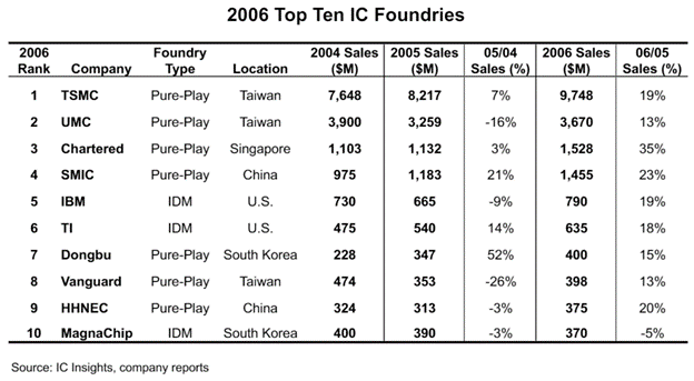
Figure 11: Top 10 IC Foundries
They also coined the term “GigaFab” for the two 300-mm fabs, with a total capacity of 271,000 300-mm wafers in 4Q06. “These ‘GigaFabsSM’ are centers of our unceasing effort to improve manufacturing excellence and to continue to deliver breakthroughs. Our gigafabs attain lower operating costs by achieving near 100 percent automation, such as real-time wafer dispatching, a search engine optimizing route for Automated Materials Handling Systems (AMHS), full automation of production wafers and non-product wafers, as well as lean work-in-progress control.” (2006 Business Overview)
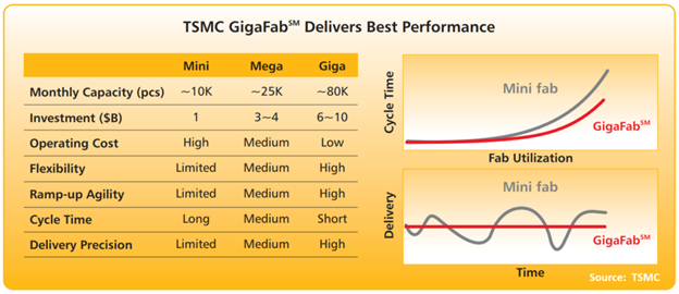
Figure 12: TSMC GigaFab Delivers Best Performance
The next full node was 65 nm, and there we found an interesting example of foundry–client customization. In addition to an Altera FPGA, we identified a Texas Instruments (TI) baseband processor fabbed by TSMC. While the back-end stacks are similar, we see notable differences in the transistor structure.
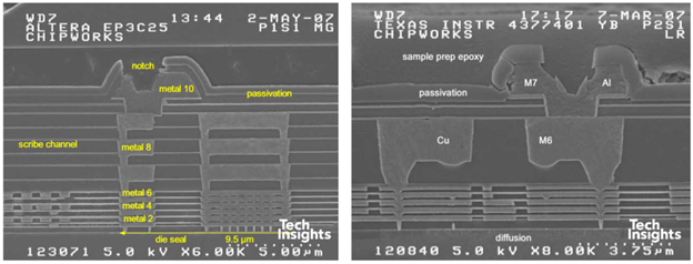
Figure 13: Cross-sections of die seals of (left) Altera FPGA and TI Baseband processor
The TI part has a noticeably thicker (1.6 µm) top copper layer, suitable for RF features such as inductors, whereas the FPGA is ~0.85 µm; the lower metal pitches were smaller to match TI’s 65-nm process. Other than that, the lower metal/dielectric stacks are similar. This processor was made for Nokia phones, and TI used their own fab, UMC, and TSMC to produce chips; we presume quite a high-volume part! Here is a look at the transistors.
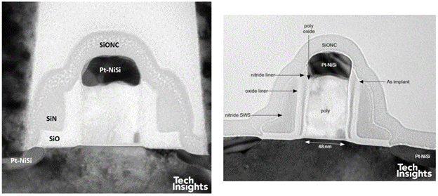
Figure 14: Cross-sections of transistors of (left) Altera FPGA and TI baseband processor
The Altera device follows the trend of 90- and 80-nm transistors, with a switch to platinum-doped nickel silicide and a modified (possibly stressed) contact etch-stop layer (CESL). The TI transistor incorporates their differential offset spacer (DOS) technology and the L-shaped spacers [5] retired by TSMC at 110-nm. Both substrates were rotated 45o to give <100> channels.
A 55 nm, 10% shrink process was announced in 2007, but we do not seem to have analyzed any contemporary products from that time. Of course, development had been ongoing on the next process generations, and both conventional (SOI) and high-k metal-gate (HKMG) 45-nm papers were presented at IEDM 2007 [6, 7, 8].
Commercially, 2007 saw the final divestment of Philips’ TSMC stock, arguably the most successful joint venture in the semiconductor industry to that time—Philips’ initial investment of ~$13 million grew to over $10 billion in the 20 years of the partnership. Capacity also increased from ~7.1 million to ~8.3 million wafers (8-inch equivalent), two-thirds of that in the two 300-mm fabs.
As TSMC developed their 45-nm technology, Intel launched their 45-nm HKMG process, a seminal change in transistor structure, eliminating the polysilicon gate and replacing it with a sophisticated metal stack.
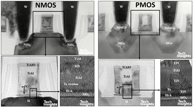
Figure 15: Cross-sections of Intel 45-nm transistors
TSMC took a more conservative route to 45 nm, though with significant changes—immersion lithography, extreme low-k (ELK), and stressed transistors. It appears that these changes slowed down the introduction of 45 nm, to the extent that the node was effectively passed by, and full ramp-up was on the planned half-node at 40 nm.
From commentary at the time, it was not just the introduction of new process steps that caused problems, it was also process/layout interactions. “Okay, in this generation what we find what’s important that design layout styles because in our products we do see the design has a — because a different product has a different yield showing, and it ranges quite widely, and we find as for those products that yields low is mainly because of the design layout dependence. What do we call design for manufacturing? That is in plain English is when the design cannot be completely described by the design rule, we have an additional algorithm software to optimize the layout so that it gets the best yield.” (Mark Liu, 2Q09 analyst call). New metrology also had to be installed and run up.
The Great Recession also hit in 2008–2009; the worldwide IC market declined 10% in 2009, though with a huge bounceback in 4Q09 of 47% compared with 1Q09. The effect can be seen quite starkly in TSMC’s 65/40nm revenue plot.
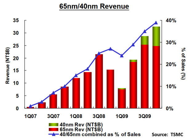
Figure 16: 65nm/40nm Revenue
The 40-nm process incorporated the 45-nm process changes, though with minimal shrink on the published 45-nm dimensions [6]. It was initially offered in three versions, low power (LP), general purpose (GP), and high performance (GS), with an ultra-low performance variant added later.
Analysis of all three processes showed that GS used dual-stress CESL nitride (DSL: tensile stress for NMOS, compressive for PMOS) and embedded SiGe source/drains for additional PMOS compressive stress. The GP process also used DSL, but a lower Ge content (19% vs. 26%), and the LP continued the use of the DOS spacer and <100> channels but no DSL or e-SiGe. All versions seemed to utilize ELK (likely Black Diamond II) for the lower metal layers.
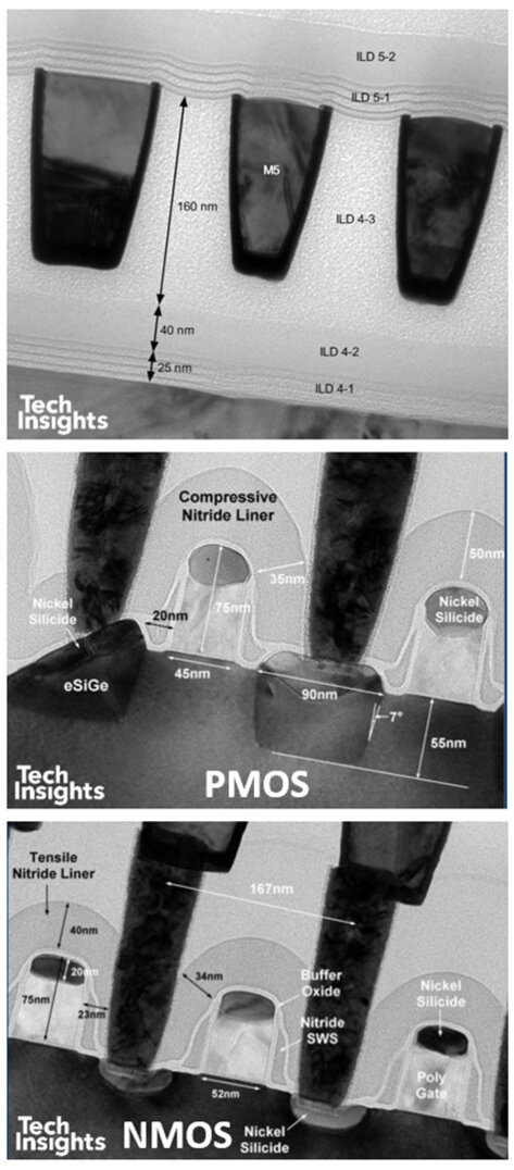
Figure 17: Cross-sections of 40-nm GS Altera FPGA ELK dielectric (top) and transistors
By the end of 2009 TSMC had more than 400 customers and manufactured more than 7000 products for them in the year. Shipments had increased over the decade from 1.8 million wafers (8-inch equivalent ) to 7.7 million in 2009, and capacity expanded from 1.9 million to 10 million wafers per year, reflecting the expansion of the 300-mm fabs to Fab 12, Phase IV and Fab 14, Phase III. As a result, revenue had grown to ~NT$ 296 billion from ~NT$ 73billion—over 400% growth in the 10 years.
Phase 5 – HKMG & Expand, Expand, Expand
To be continued…
References
- F.C. Tseng, “Foundry Technologies”, IEDM 1996, pp. 19–22
- M.H. Chang et al., “A Highly Manufacturable 0.25 µm Multiple-Vt Dual Gate Oxide CMOS Process for Logic/Embedded IC Foundry Technology”, VLSI Technology 1998, pp. 150–151
- C.H. Diaz et al., “A 0.18 µm CMOS logic technology with dual gate oxide and low-k interconnect for high-performance and low-power applications”, VLSI Technology 1999, pp. 11–12
- M. Naik et al., “Process Integration of Double Level Copper-Low k (k= 2.8) Interconnect” IITC 1999, pp. 181–183
- B. Hornung et al., “A High Performance 90 nm Logic Technology with a 37nm Gate Length, Dual Plasma Nitrided Gate Dielectric and Differential Offset Spacer” VLSI Technology 2003, pp. 85–86
- K-L Cheng et al., “A highly scaled, high performance 45 nm bulk logic CMOS technology with 0.242 μm2 SRAM cell”, IEDM 2007, pp. 243–246
- S, Fung et al., “45nm SOI CMOS Technology with 3X hole mobility enhancement and Asymmetric transistor for high performance CPU application”, IEDM 2007, pp. 1035–1037
- H.T. Huang et al., “45nm High-k/Metal-Gate CMOS Technology for GPU/NPU Applications with Highest PFET Performance”, IEDM 2007, pp. 285–288