Logic Blog
A Trip Down TSMC Memory Lane – Part 1

Dick James
A few months ago we published a blog on MOS process history, triggered by Pat Gelsinger’s keynote at the Intel Innovation Days in November last year, and while at the start it was generic, when we got to 90 nm we became specific and showed Intel devices.
That prompted us to look back at one of the other companies that has made huge changes in the semiconductor industry and ecosystem, namely Taiwan Semiconductor Manufacturing Company, more universally known as TSMC.
Phase 1 – Start-up
A bit of history to start – formed in 1986 with Morris Chang as Board Chairman, shortly after his move to Taiwan to head up their Industrial Technology Research Institute (ITRI). Start-up funding was $48M from Taiwan’s Executive Yuan Development Fund (48.3%), N.V. Philips (27.5%), and the remainder from other Taiwanese companies who had their arms twisted by the government. Two more rounds of funding of $29M and $205M came in 1988, giving a total of $282M.
Production started in the following year in 1987, initially in a leased ITRI 6” fab, using 2- and 3.5 µm technologies from ITRI. This was quickly followed by a customized 3.0 µm technology for Philips, which was probably their first serious volume process.
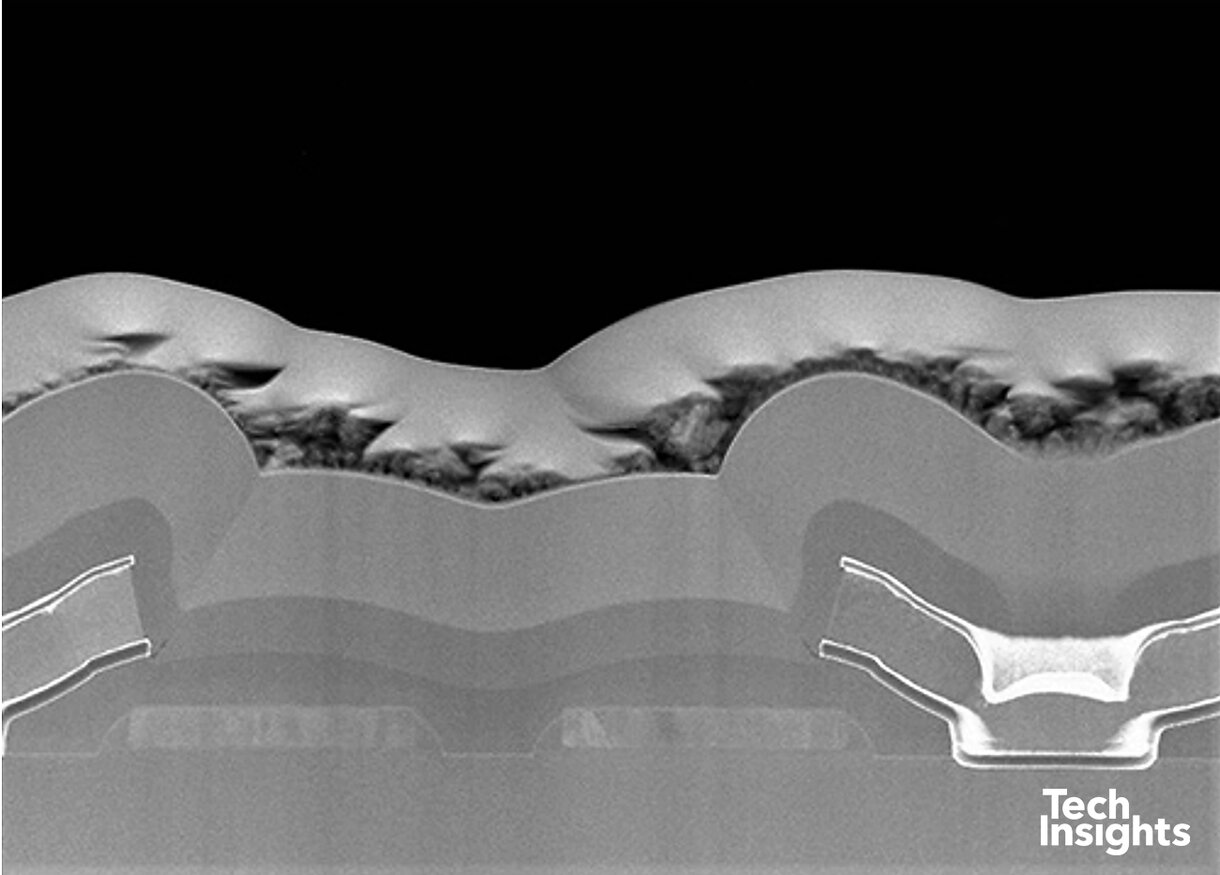
Fig-1-TSMC-3-µm-a
As you can see, it was a single-poly, single-metal process; we have marked up the image since you probably have to be over 60 to recognise this technology! This was rapidly followed by a 1.5 µm technology in 1988.
The rapid sequence of process development is well shown in this plot from their website;
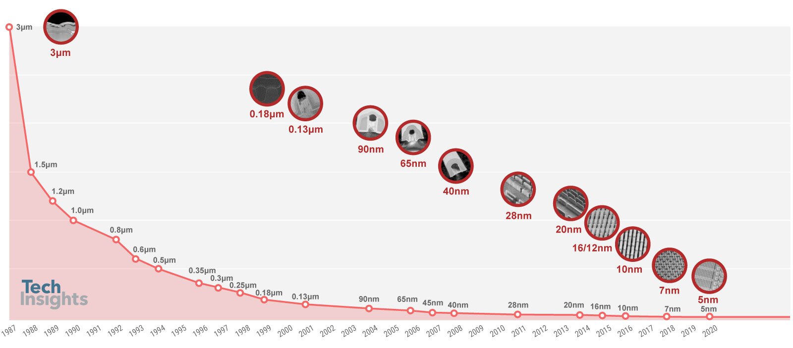
Fig-2-Process-Technology-Nodes_20210603
TSMC went public in 1994, and by that point they had evolved to a 0.6 µm 3-metal logic process, as well as a 2-poly, 2-metal mixed-signal version and a 1.0 µm BiCMOS technology. They also had Fabs IIA and IIB operating, with an 8” Fab III being commissioned. Between 1990 – 1994 they shipped 2.5M wafers, and sales went from NT$ 2.2B to 19.3B, so the foundry model was definitely taking off.
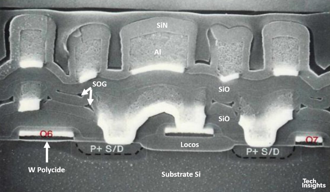
Fig-3-Cross-section of Altera 0.6 µm EPLD
The Altera EPLD above is only a two-metal version of the 0.6 µm process, but we can see that planarization (such as it was) was achieved by a combination of flowed glass (phosphosilicate or boro-phosphosilicate glasses – PSG or BPSG), spin-on glass (SOG), oxide deposition and etch-back. This was good up to three metal layers, but above that lumpiness got too much and the step coverage of the aluminum just could not cope. The ICE assessment was that metal in the contacts was thinned by up to 75%.
(ICE – Integrated Circuit Engineering, was a Phoenix-based company that was absorbed by Chipworks in 2001, and their reports are fortunately still available in TechInsights. We had to search way back to find some of these records!)
We had also evolved to tungsten silicide on the gates, but not source/drains, and locos was still the dominant method of device isolation.
Phase 2 – Expansion and Catch-up
1995 saw the opening of 8” Fab III, and the introduction of tungsten plugs. The plugs were formed by deposition and etch-back, even though IBM had developed CMP (chemical-mechanical planarization) some years earlier. The use of plugs improved planarization and enabled more metals:
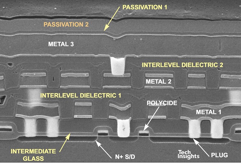
Fig-4-Cross-section of Altera 0.5 µm EPLD
By 0.35 µm (1997) TSMC had adopted CMP and titanium silicide was used on the source/drains, though tungsten stayed on the gates.
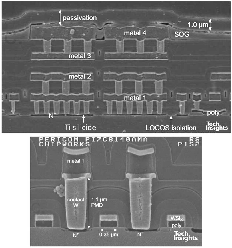
Fig-5-Cross-sections of Pericom 0.35 µm PCI bridge
Also in 1997, TSMC started the habit of “half-node” processes, with the launch of 0.3 µm processing; and the opening of fab V. The following year we saw the first 0.25 µm product – as we can see, we have full implementation of CMP with six metals in this part, full self-aligned titanium silicide (Ti salicide), and the introduction of shallow trench isolation (STI).
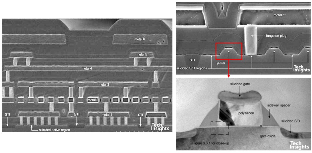
Figure 6: Cross-sections of Philips 0.25 µm graphics processor
Business-wise, in 1998 they achieved NT$ 50 billion revenue, shipping 1.2M 8” equivalent wafers, in what was a recession year for semiconductors, and the Wafertech fab in Oregon began shipping wafers.
Recently Shang-Yi Chiang, former VP of R&D at TSMC, contributed his oral history to the Computer History Museum, and he stated that their 0.25 µm process used fluorosilicate glass (FSG) as a form of low-k dielectric, but our reports have no record of that. He also said that getting that node released was extraordinarily difficult, but they made it on schedule.
Production also started of the 0.22 µm node in 1998; as expected, this looked very similar to the 0.25 µm generation, with tighter metal pitches, but there was a change in the transistor structure:
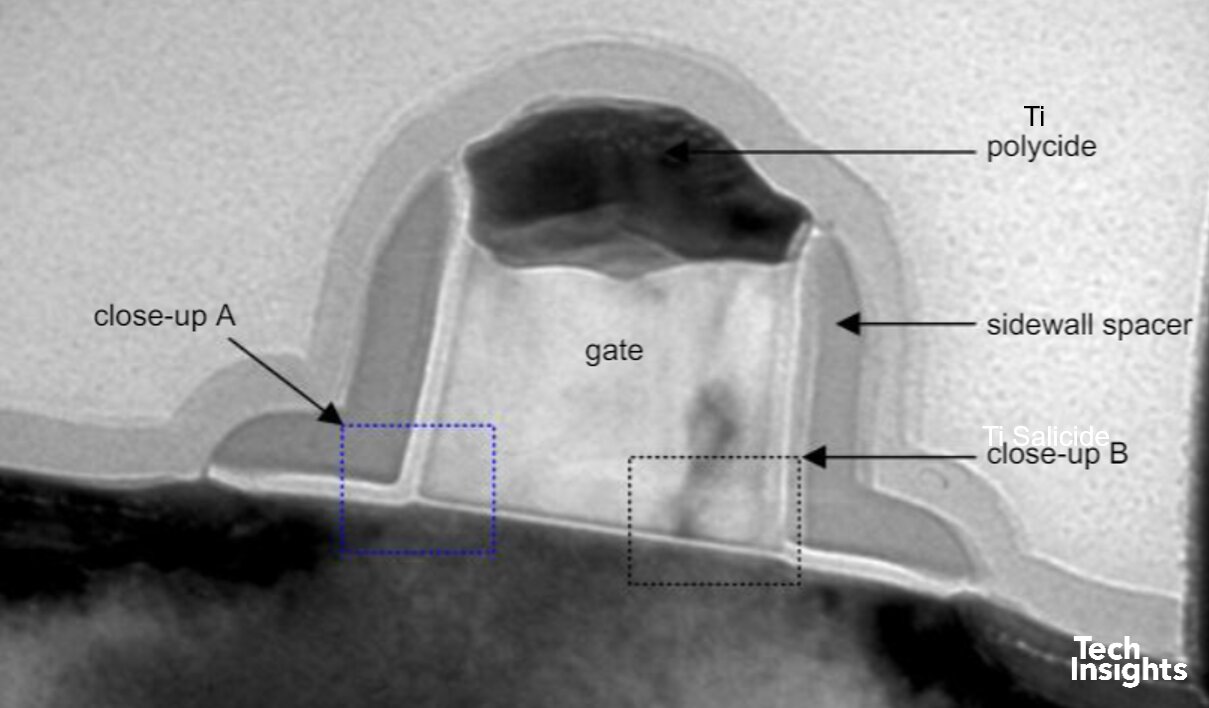
Figure 7: Cross-section of transistor from Altera 0.22 µm FPGA
Ti salicide was still used, but we now have L-shaped sidwall spacers instead of triangular. Gate length was 0.16 µm, so we are now in the era where node designations start to get meaningless – down to 0.25 µm, gate length was a fairly reliable indicator of manufacturing generation.
At 0.18 µm (180 nm) in 2000, we noted the change in the back end, and identified FSG in the dielectric stack. (FSG has a dielectric constant of ~3.6, vs ~4.0 for SiO2.) That year also saw the opening of fab VI, which also had a 300-mm pilot line in-house.
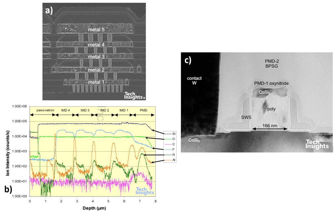
Figure 8: 180 nm Lucent DSP a) cross-section of metal/dielectric stack b) SIMS analysis of dielectric stack c) cross-section of transistor
We still have the L-shaped spacers in the transistor stucture, but there is a switch to cobalt salicide – and gate length was ~130 nm! The Lucent part shown above has a five-metal stack, but we also analyzed parts with seven metal layers.
The millenial year was a boom year for TSMC, with sales increasing 127% on 1999, giving an annual compound growth rate of 50% for 1992 – 2000.
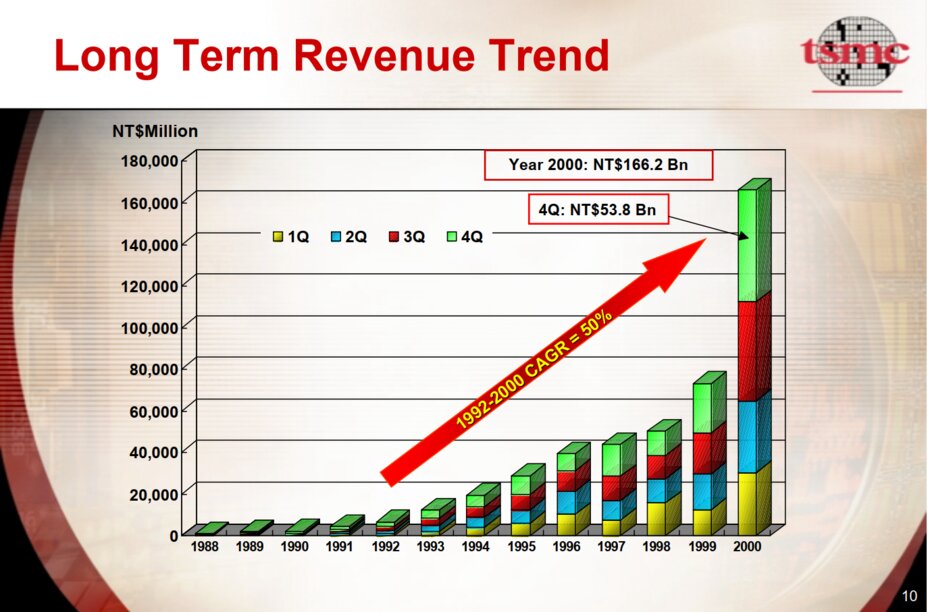
Fig-9-TSMC-1992-2000
A 150-nm generation was also launched that year,continuing the pattern of half-nodes. In the background R&D was developing the 130-nm (copper) process, and also setting up 300-mm processing, while 300-mm Fab 12 in Hsinchu and Fab 14 in Tainan were under construction.
Phase 3 – Drawing Level – and Even (Briefly) Ahead
To be Continued…