Posted: April 11, 2019
Contributing Author: Dick James, Jeongdong Choe
On the Sunday evening at IEDM last year, TechInsights held a reception in which Arabinda Das and Jeongdong Choe gave presentations that attracted a roomful of conference attendees. Arabinda was first up, giving a talk on the “10-year Journey of Apple’s iPhone and Innovations in Semiconductor Technology”, followed by Jeongdong discussing “Memory Process, Design and Architecture: Today and Tomorrow”.
Arabinda gave a broad-brush look back at the sequential development of the iPhone and its feature components – we tend to forget that the first one had no camera, fingerprint sensor, face recognition, etc., so it was definitely a trip down memory lane.
Jeongdong presented a review of the latest memory technologies seen by the reverse engineering specialists, summarising their recent analyses in a fair amount of detail, and which I’d like to go through in this article. Jeongdong is a Senior Technical Fellow at the company, and their subject-matter expert for memory technology. Before joining TechInsights, he worked as a Team Lead in R&D for SK Hynix and Samsung advancing next-generation memory devices, so he knows whereof he speaks.
NAND Flash Technology
We started with a look at NAND flash, with the market shares of the top six manufacturers given as Samsung 36%, Toshiba 19%, Western Digital (WD) 15%, Micron 13%, SK Hynix 11%, and Intel 6%, as of November 2018.
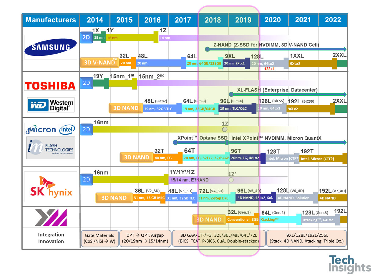
Jeongdong generates road-maps for memory every year, and below is the updated one for NAND flash. You can see that we are now into the era of 1z-nm planar flash (probably 13-14 nm, seeing as 1y was ~15 nm), and ~96 layers of 3D flash, with quadruple-level cells. The roadmap is based on published predictions, but I find it hard to believe that in a mere three years we will be getting to 200+ layers.
At the bottom of the figure is the technology evolution over the last few years, starting with the transition of the control gate from silicides to tungsten in planar devices; then we move from double patterning to quadruple patterning, as we get below 20 nm feature sizes. We see the widespread adoption of air gaps (actually, Micron started that at the 25-nm generation), and as the 15/16 nm planar parts see full production, the 3D/V-NAND products are launched. Those use two storage technologies, charge-trap (storing the charge on a silicon nitride layer – Samsung, Toshiba/WD, and SK Hynix), and floating gate (Micron/Intel).
9X Layer 3D NAND Analysis - Learn More
Download our overview of 3D NAND Analysis, complete with a market overview, NAND technology roadmap, die images, and an outline of the different analytical methods we can apply to these products.
Micron/Intel also used a different layout philosophy which gave a greater areal data density; they engineered the stack to have the drive circuitry under the array, saving peripheral area, and making the die smaller – dubbed by them as CMOS-under Array (CuA). Their 64-layer product is a 2x 32 stack, and the 96-layer uses 2x 48-layer stacks.
Looking to the future, the roadmap shows up to 256 layers, and planar will fade out except for niche applications. “4D NAND” appears to be the SK Hynix version of CuA, and Xtacking is the YMTC (Yangtze Memory Technologies Co.) process of stacking CMOS over the array to save area.
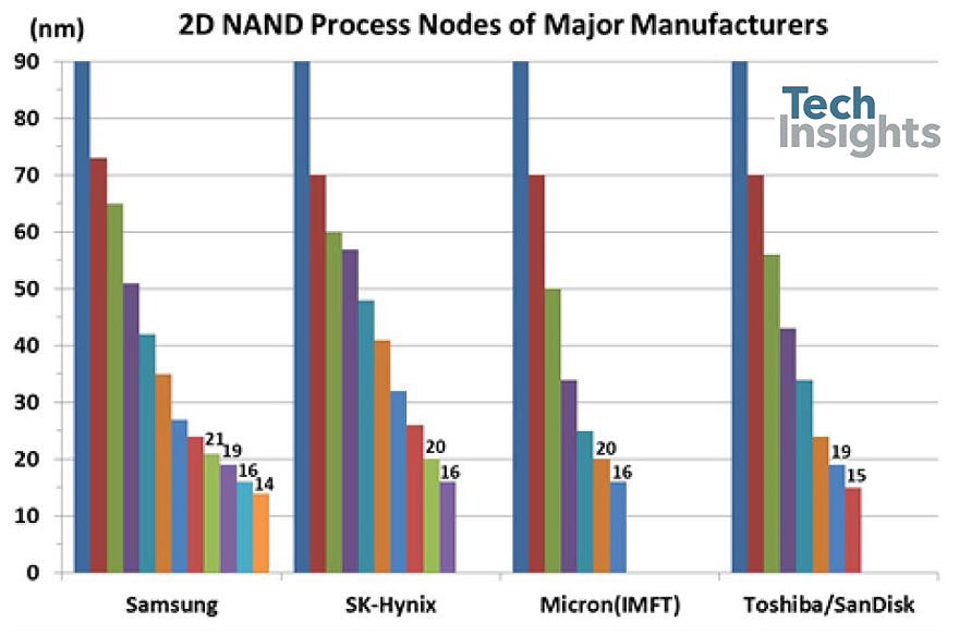
Tracking the planar devices, we have this sequence from the major manufacturers:
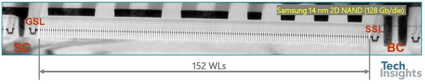
The smallest half-pitch seen so far is the Samsung 14-nm 128-Gb die, with a block size of 152 cells:
3D NAND: 64L & 72L (256 GB & 512 GB)
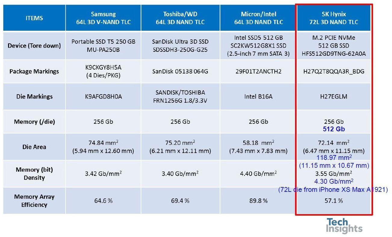
Switching to 3D-NAND, Jeongdong showed us this summary of recent 64- and 72-layer devices:
We can see how the CuA in the Intel part improves the array efficiency to almost 90%, giving the smallest die of the 256-Gb group. The SK Hynix 512-Gb die from the iPhone XS Max has almost the same memory density, an impressive improvement from the 256-Gb part.
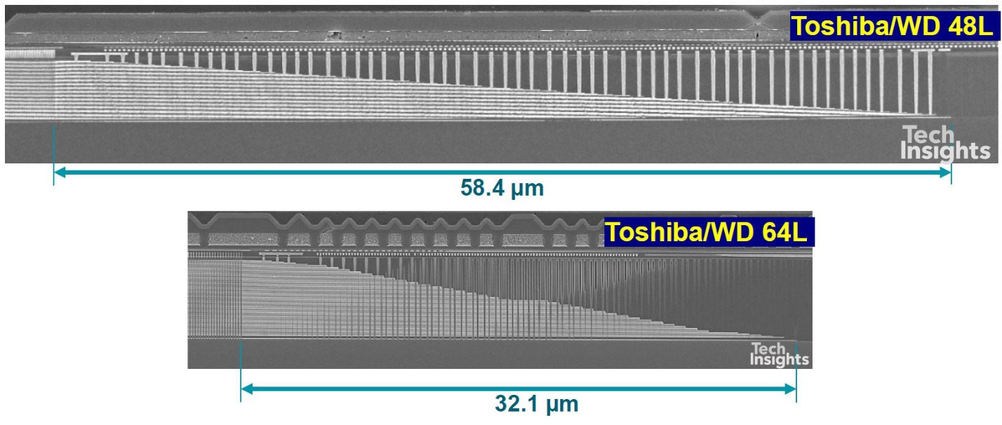
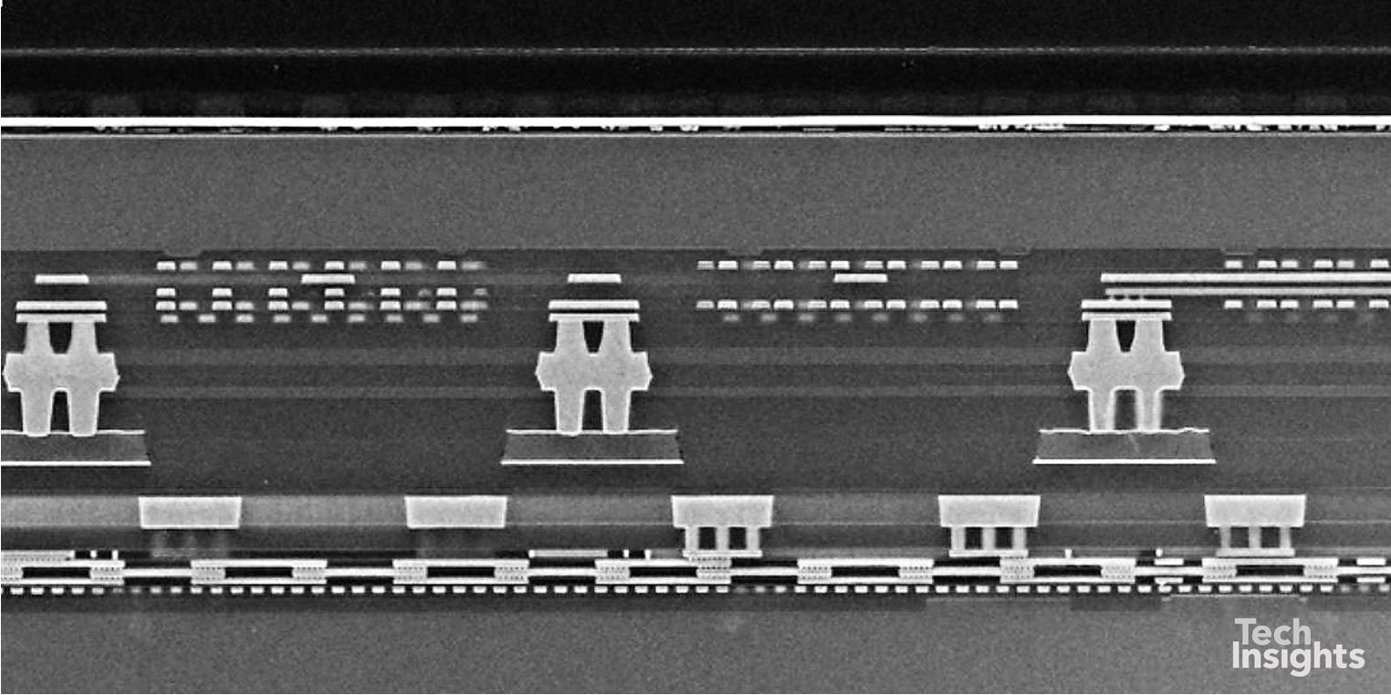
One of the developments made in the transition from 48-layer to 64-layer technology is in the etching of the “staircase” that is used to contact the wordlines in 3D-NAND devices. For example, in the Toshiba/WD parts, the width of the staircase has shrunk by 45% due to etch process improvements and trimming mask changes.
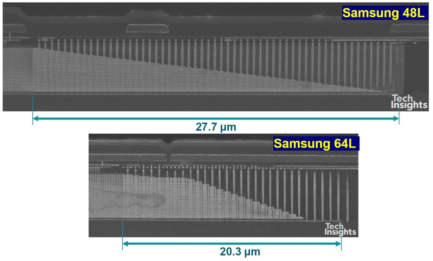
This is not insignificant, even after the shrink the staircase takes up 0.82% of the die area. Similarly, Samsung achieved a 27% width reduction, finishing with a 0.44% area penalty for the staircases.
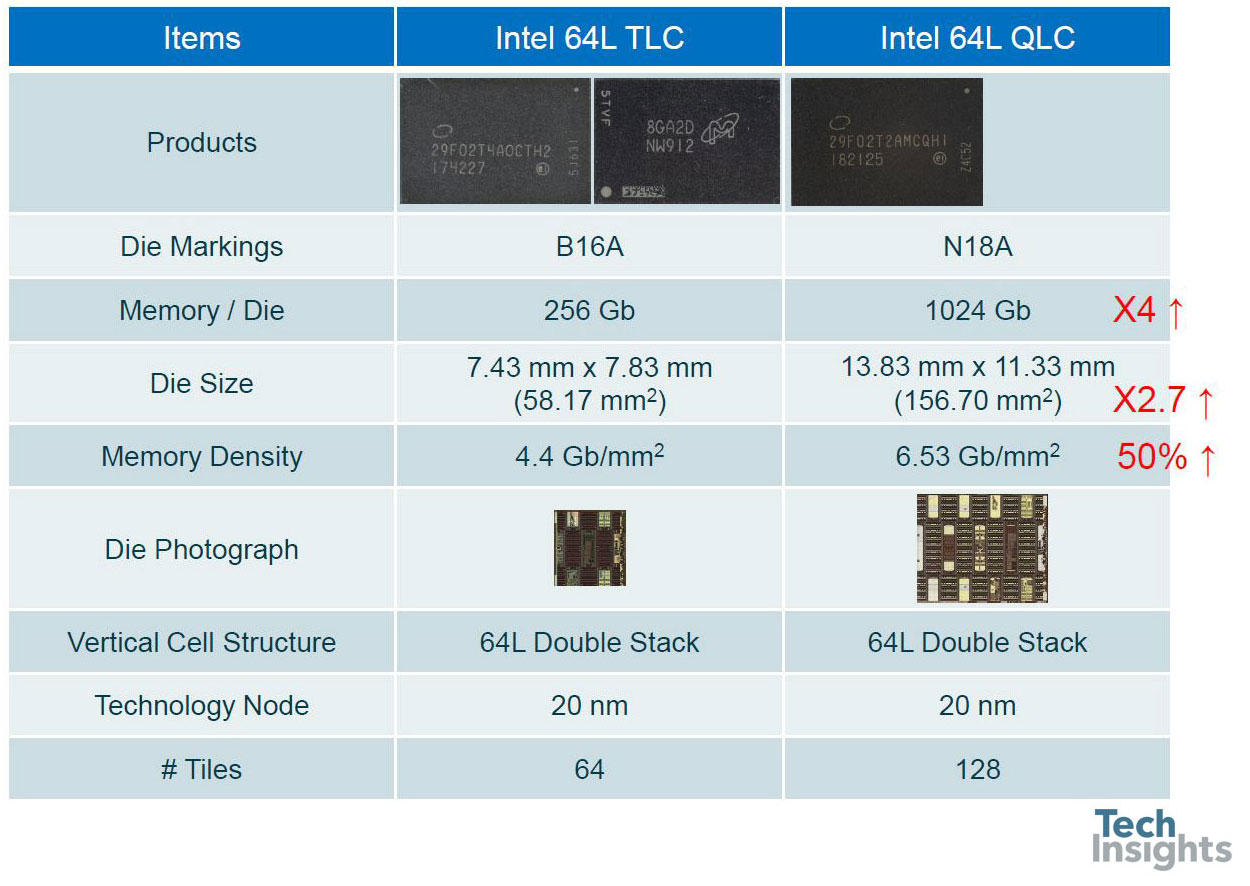
Intel 3D FG NAND QLC (64L): First 3D QLC!
We also had the opportunity to compare Intel/Micron’s tri-level and quad-level cell parts; even though they are both 20-nm, and both 64-level, the bit density goes from 4.4 to 6.5 Gb/mm2, an increase of almost 50%. We are now in the era of the terabit die, Micron has just announced 1-TB micro-SD cards with eight 1-Tb dies inside!
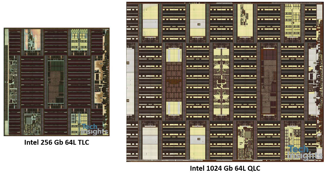
The transistor-level die photos are tiny in the above slide, but they do zoom out quite well:
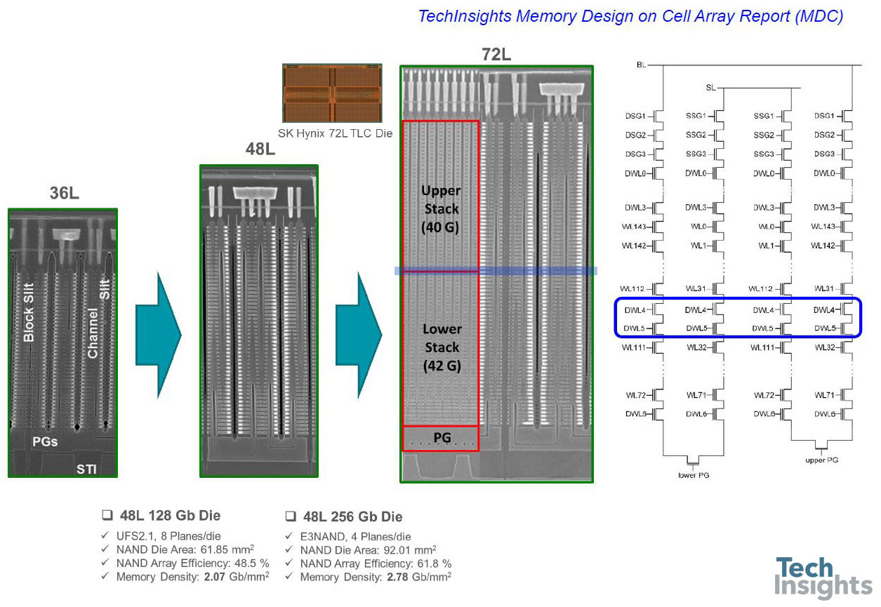
SK hynix 72L P-BiCS
We can clearly see the density of circuitry underneath the array in these shots. Next up was a look at the SK Hynix 3D-NAND, which uses a folded structure.
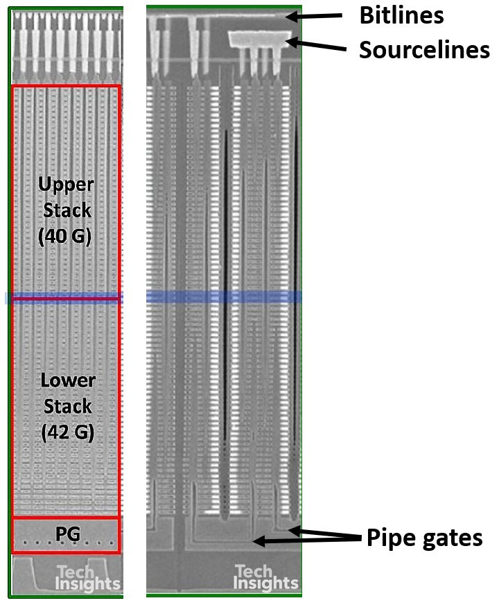
If we look closely we can see the evolution in the stack from 36 – 48 – 72 layers. The 36L device only has one pass gate, whereas the 48L and 72L have two pass gates, allowing common bitlines and sourcelines for two chains of cells. The centre image of the 72L stack is a little confusing, since it has two orthogonal images glued together – the right side is a section parallel to the bitlines, and the left perpendicular to them. If we look at the separated images, the holes in the PG region show that the left section is through the lower of the two pipe gates, and at the top the individual bitlines are visible.
The upper and lower stacks refer to the two-stage construction of the 82-gate stack. Jeongdong did not go into the details of this in this talk, but he posted a blog on EETimes last June that clarifies that the channel holes are formed with a two-step etching process. The estimated process sequence is:
- Pipe gate mold formation (lower portion)
- Channel etching (lower portion, 42 gates)
- Sacrificial layer filling into holes
- Mold formation (upper portion)
- Channel etching (upper portion, 40 gates)
- Sacrificial layer removal
- Channel formation
The slits and sub-slits are formed by one-step etching of the whole stack. In the circuit schematic above, the blue outline shows the location of two dummy wordlines between the top and bottom stacks, marked by the blue line in the cross-section.
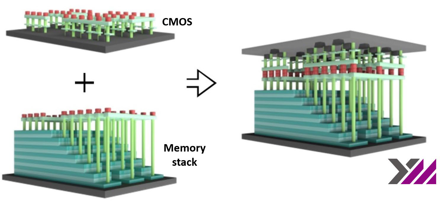
The last NAND device discussed was the YMTC 64L part displayed at the Flash Memory Summit last year. This is their second-generation 3D-NAND technology, using Xtacking to put the peripheral circuitry on top of the memory array instead of underneath it. YMTC uses face-to-face wafer bonding:
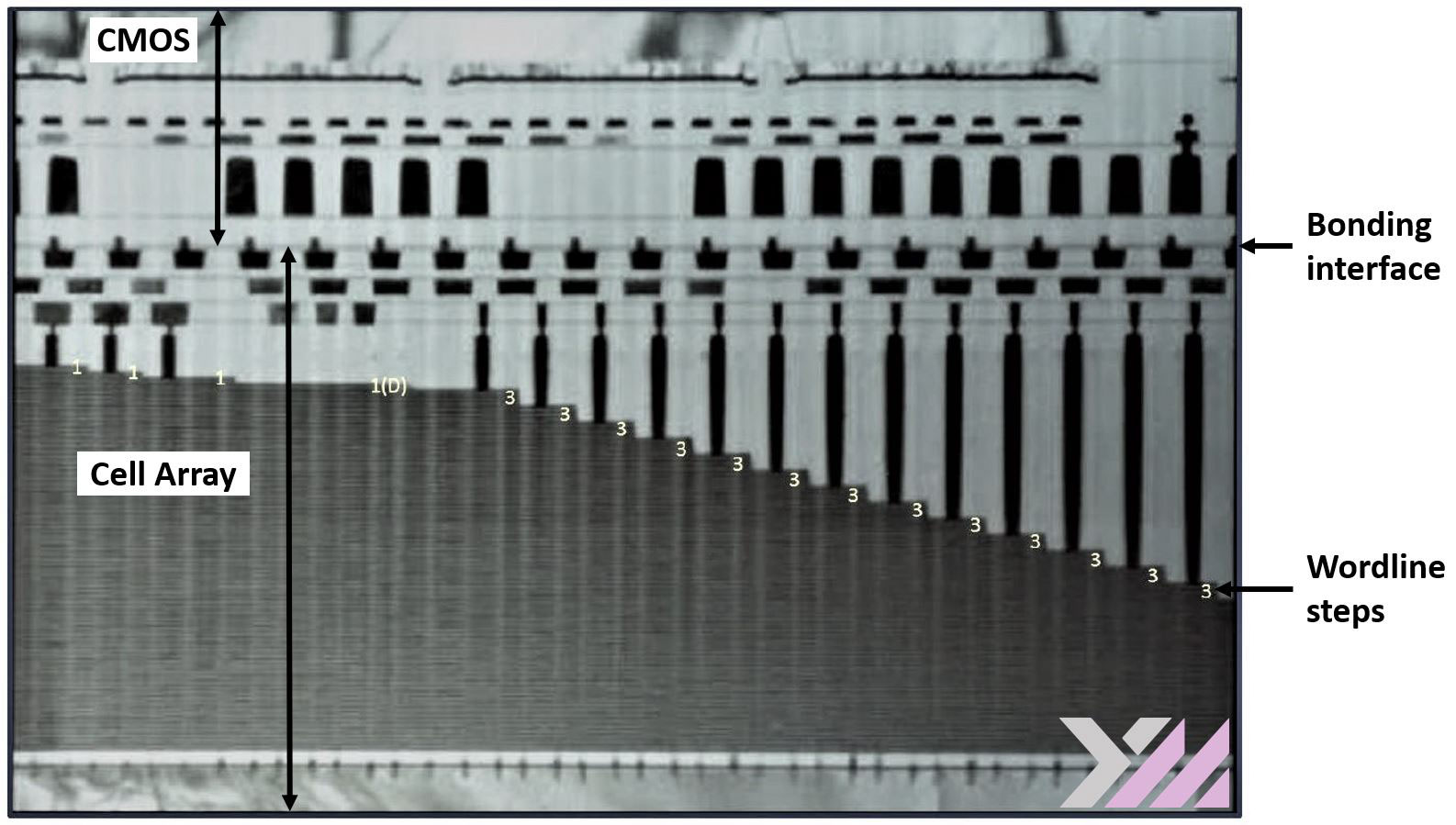
I annotated the image that Jeongdong used, to try and clarify what we are looking at:
Technology Innovations on 3D NAND (Today)
We have the typical staircase at the edge of the array, and they have helpfully added the number of wordlines per step, showing us that there is one dummy wordline at the top, under the individually-masked select gates.
The wafer bonding gives us a total of seven damascene metal layers, three in the array, and four in the CMOS, and in the cell stack there are a total of 74 tungsten wordlines. It’s not specifically mentioned in any of YMTC’s pronouncements, but historically they have worked closely with Spansion (now Cypress) using charge-trap storage in NOR flash, so it seems likely that their 3D-NAND is also charge-trap based.
The bonding is likely the DBI® (Direct Bond Interconnect) technology from Xperi – it’s quite a fuzzy TEM image above, but it does look similar to the interface in this SEM cross-section of the Sony IMX260 stacked image sensor, which we know uses the process.
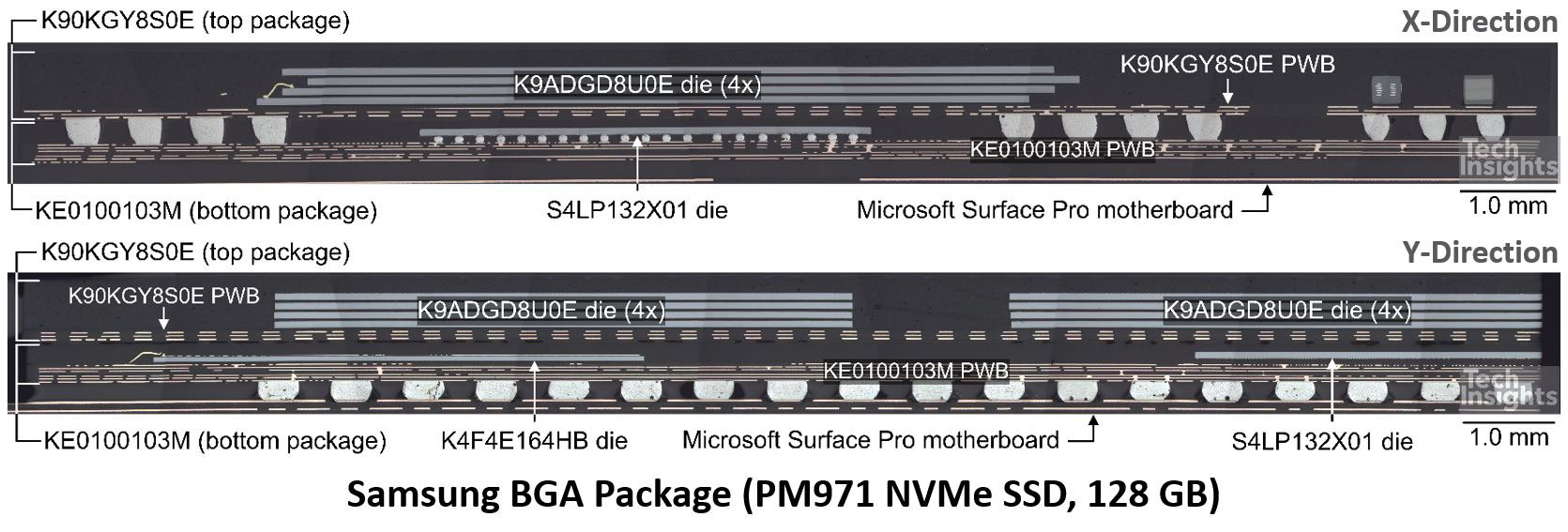
I would be remiss if I excluded an earlier slide detailing the use of Package-on-Package (PoP)for an SSD part, maybe not the first use of PoP for memory, but certainly different from the usual memory-on-APU that we are used to seeing in mobile phones. This was a Samsung single-package 128 GB SSD out of a Microsoft Surface Pro:
We have two four-stacks of 128-Gb V-NAND dies in the top part of the PoP, and in the lower part is a 4-Gb LPDDR4 DRAM and the SSD controller die.
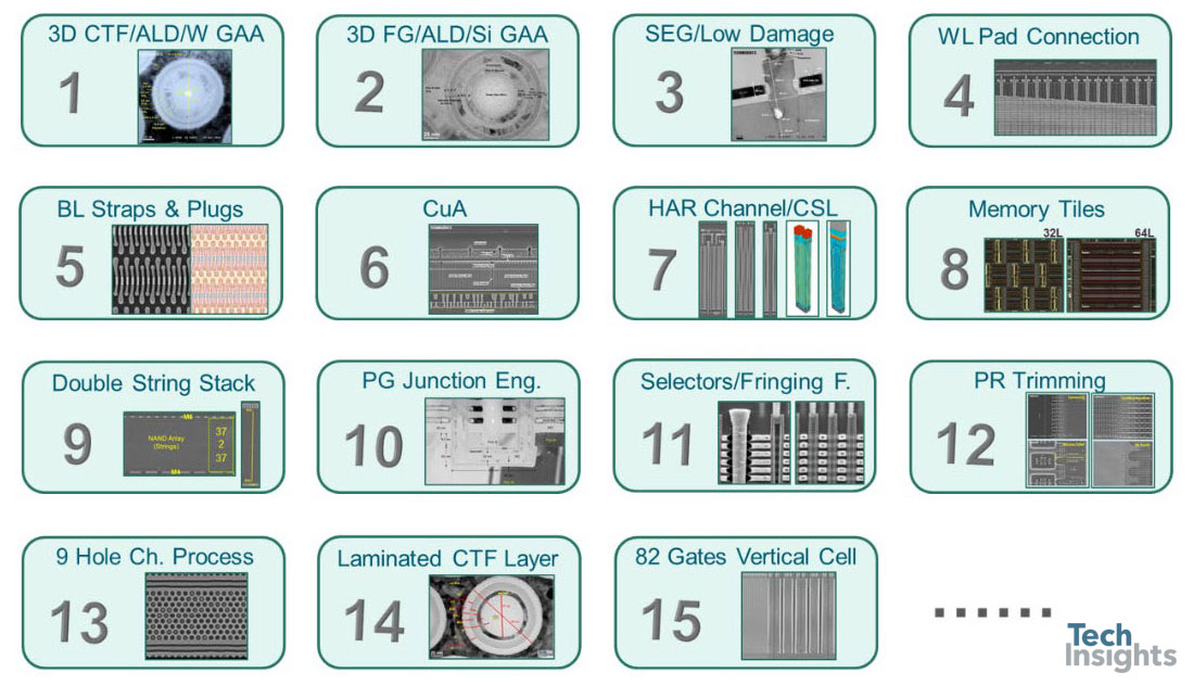
Jeongdong finished up the NAND flash section with a couple of summary slides, the first describing the innovations in 3D NAND so far. It’s a busy slide, so I won’t go through it in detail – there is a lot of innovation! Aside from the 3D stack itself, there are possibly unexpected features such as the epitaxial (SEG) transistors (Samsung), CuA and double-string stacks (Micron), and pipe gates (SK Hynix). And now we have wafer bonding!
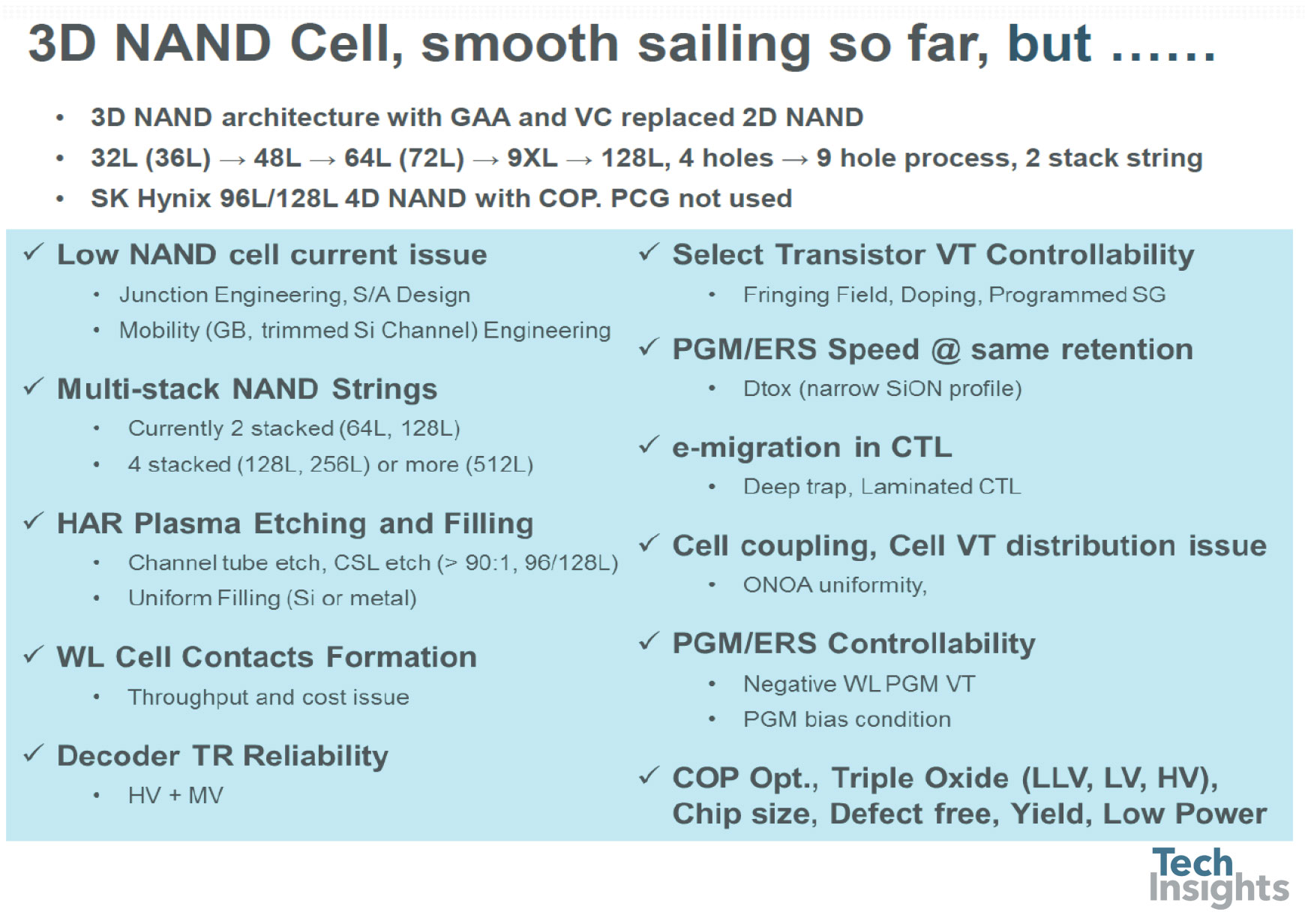
The summary slide tracked the progress so far, and raised some of the concerns for future development.
Of note to me are SK Hynix’ return to a conventional stack without the pipe gates, Micron’s (presumably) to four-stacked strings, and the generic problems of etching and filling very high aspect ratio channels.
DRAM Technology
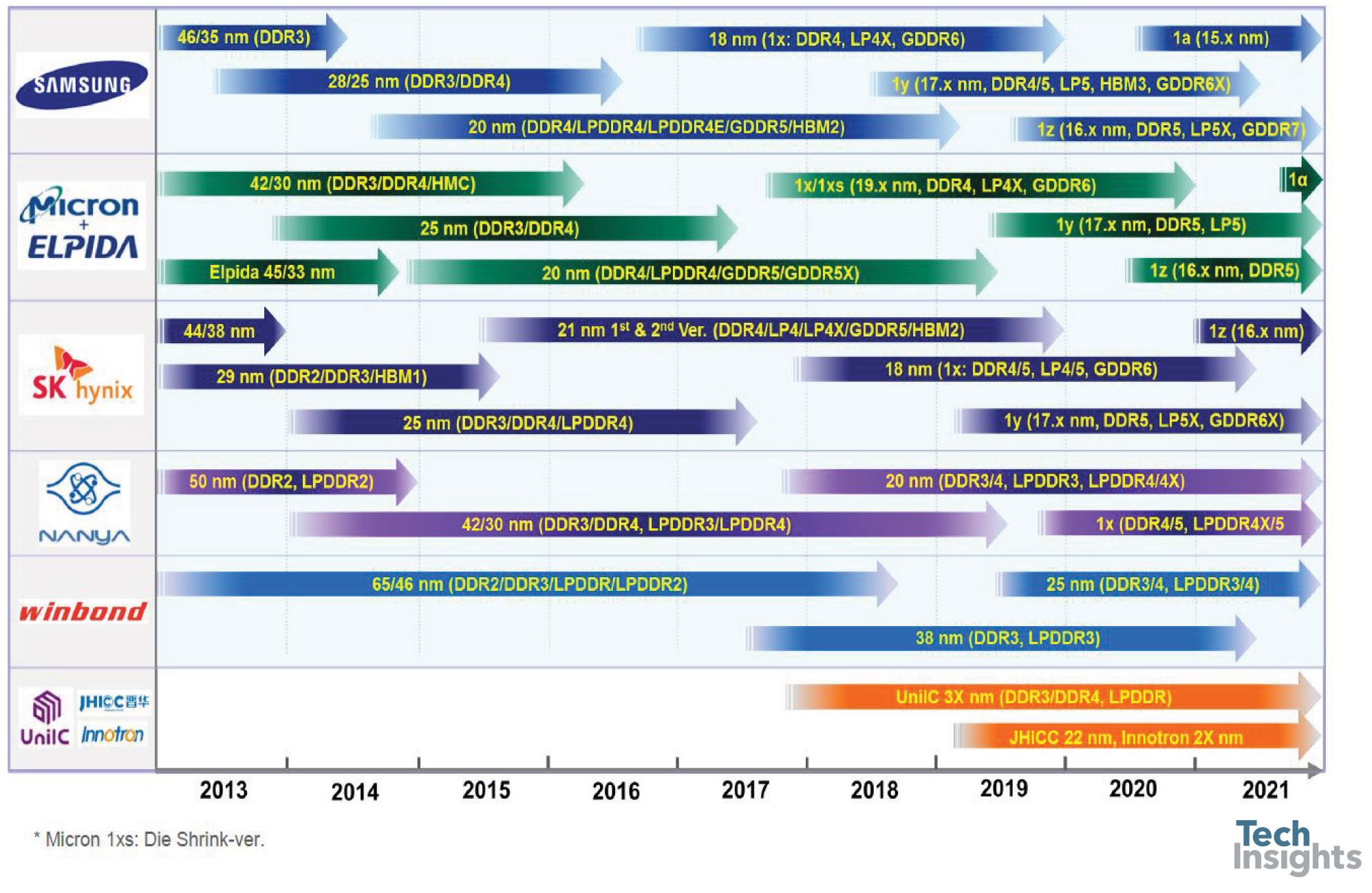
DRAM Product Roadmap Update
First up in the DRAM part of the talk was the roadmap:
We are now well into the 1x-nm generations, with 17-nm parts being introduced this year. If you believe the manufacturers, we are still on the one-year cadence for introduction of the next shrink, although the difference is smaller, now we are below 20 nm. A few years ago, I was inclined to think that we might get two generations in the 1-something nodes before the technology reached its limits, but now it seems we will see at least four, which will likely see us through to 2025 at least.
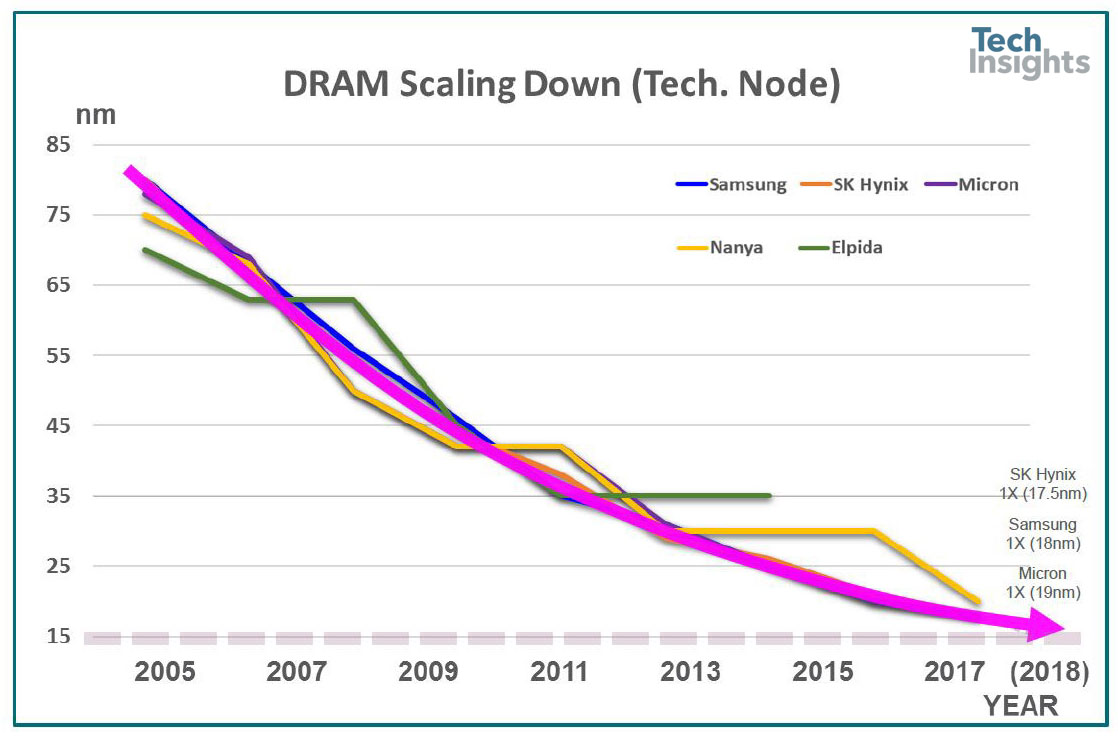
DRAM Technology Node Trend
The slowing of the shrink rate is shown by looking at the chronological trend of the nodes:
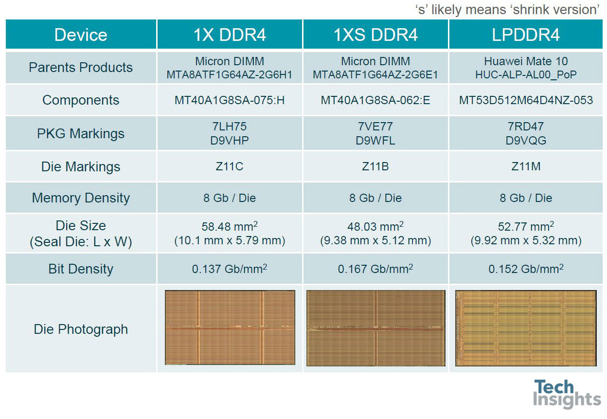
Micron 1X & 1XS nm DDR4/LPDDR4
Elpida plateaued before the Micron acquisition, as did Nanya.
Jeongdong also gave us some details of recent Micron memories, showing that in 8-Gb dies their bit density is now up to 0.167 Gb/mm2.
AMD & NVIDIA GPU Card Summary
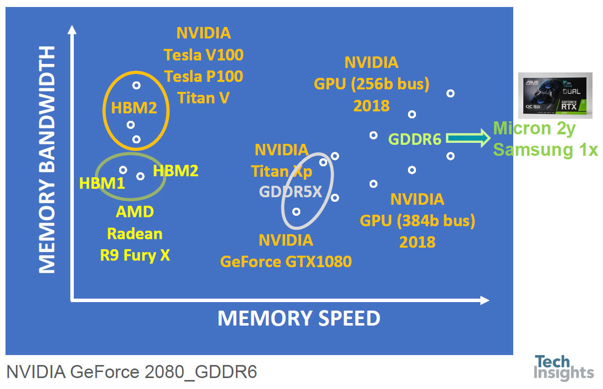
Then a look at AMD and Nvidia GPUs, illustrating the increase in bandwidth with the use of HBM (high bandwidth memory) and HBM2, and both bandwidth and speed as we move from GDDR5X to GDDR6.
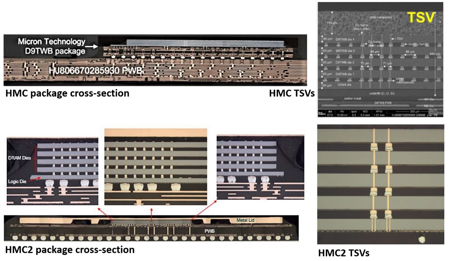
The mention of HBM brings to mind Micron’s HMC (Hybrid Memory Cube), which has now evolved into HMC2. The original HMC was used in the Intel Knight’s Landing processor, a four-stack DRAM with an IBM-fabbed controller chip at the base, connected with through-silicon vias (TSVs). HMC2 seems to have been was launched as an independent product, but still a 4-stack with controller, and both HMC and HMC2 used 30-nm class DRAMs.
Both HBM and HMC use TSVs, but they are different beasts; HMC has its controller die and is fully packaged for mounting on a PCB substrate, whereas HBM is used with a silicon interposer. However, Micron has announced that it is discontinuing HMC, so even though we got a look at it, it will not be around for much longer.
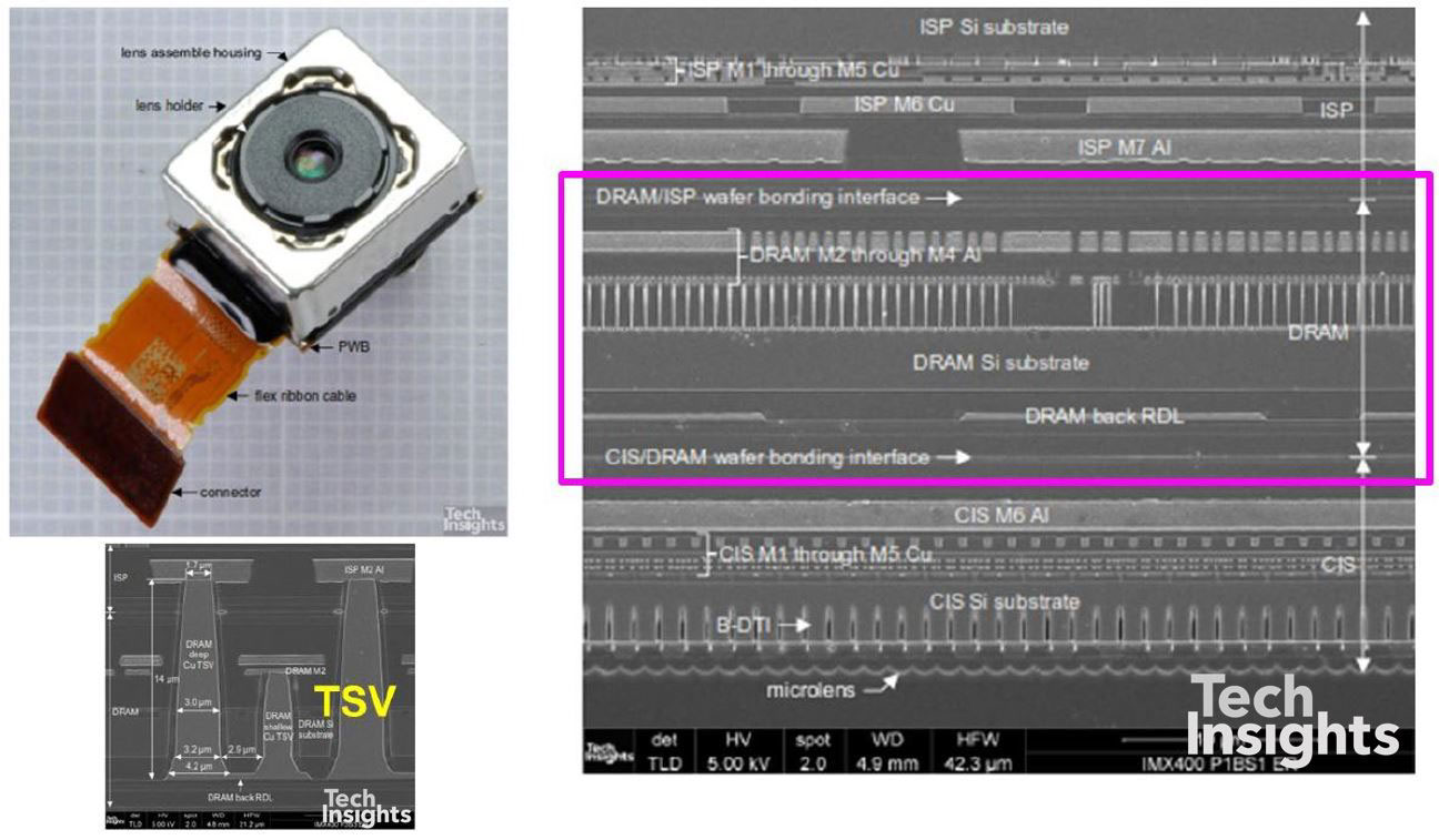
ISP/DRAM/CIS (Sony) Micron 35 nm (Likely, Elpida fab.)
The last slide of the DRAM section covered the stacking of DRAM with CMOS image sensors (CIS) and processors (ISP) for mobile phone cameras, by Sony and Samsung. In the Sony IMX400 a DRAM is sandwiched between the CIS and the ISP; the CIS is mounted face-to-back on the DRAM, which is face-to-face with the ISP. Having the DRAM in the stack allows the camera system to perform at 960 frames/sec, serious slow motion capability. The IMX400 was launched in the Sony Experia XZ phones, and we published a blog on it at the time.
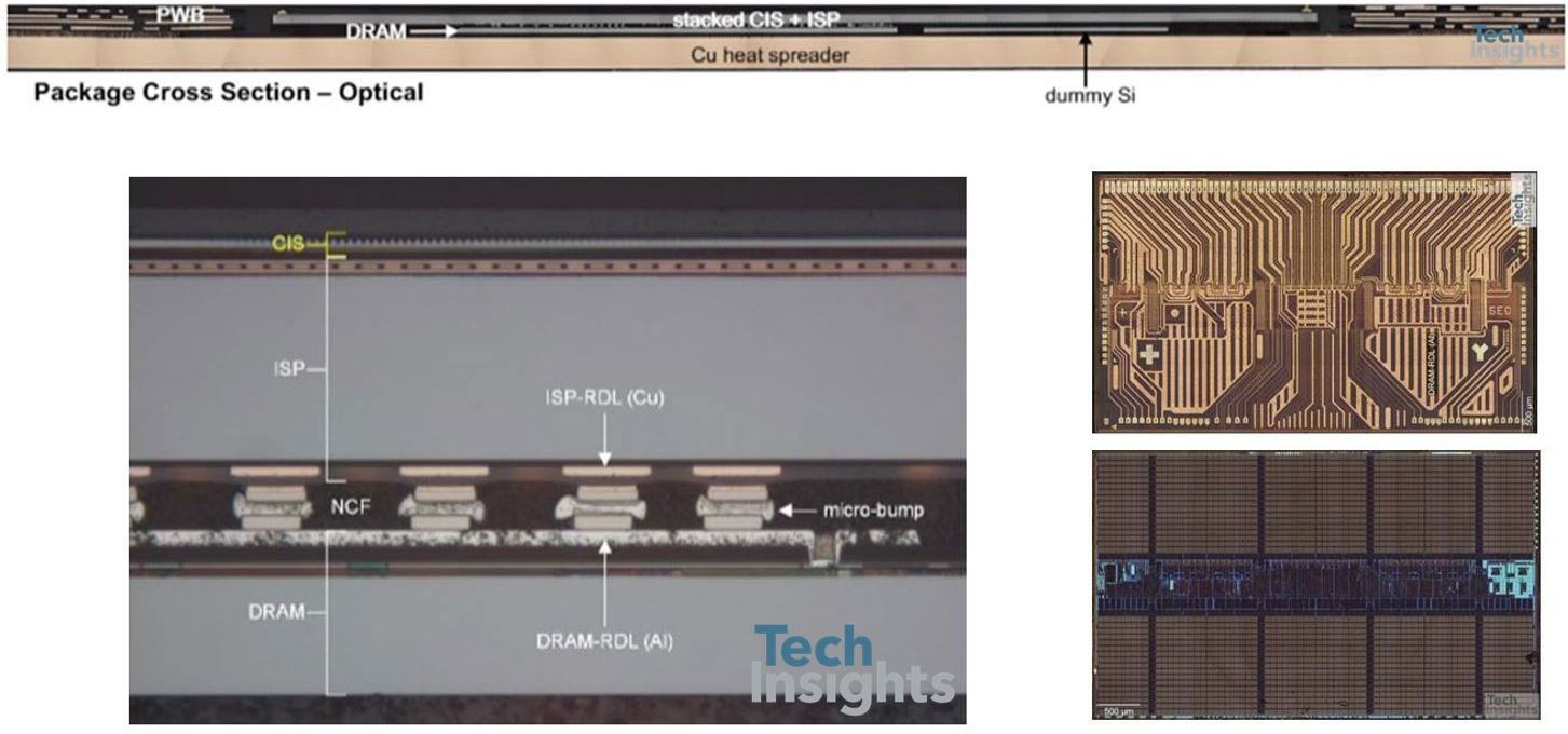
CIS/ISP/DRAM (Samsung) Samsung 2y
The Samsung S5K2L3 ISOCELL Fast imager takes a different tack – the CIS and ISP are conventionally bonded face-to-face and electrically connected using TSVs, and a standard DRAM chip is micro-bumped face-to-back on the ISP. The micro bumps connect a redistribution layer (RDL) on the DRAM to a Cu-based RDL on the back of the ISP, which routes them to TSVs, through the ISP substrate to the front metal. There is also a dummy silicon die next to the DRAM chip.
Emerging Memory Technology
Emerging Memory Mass-Products: Major Players
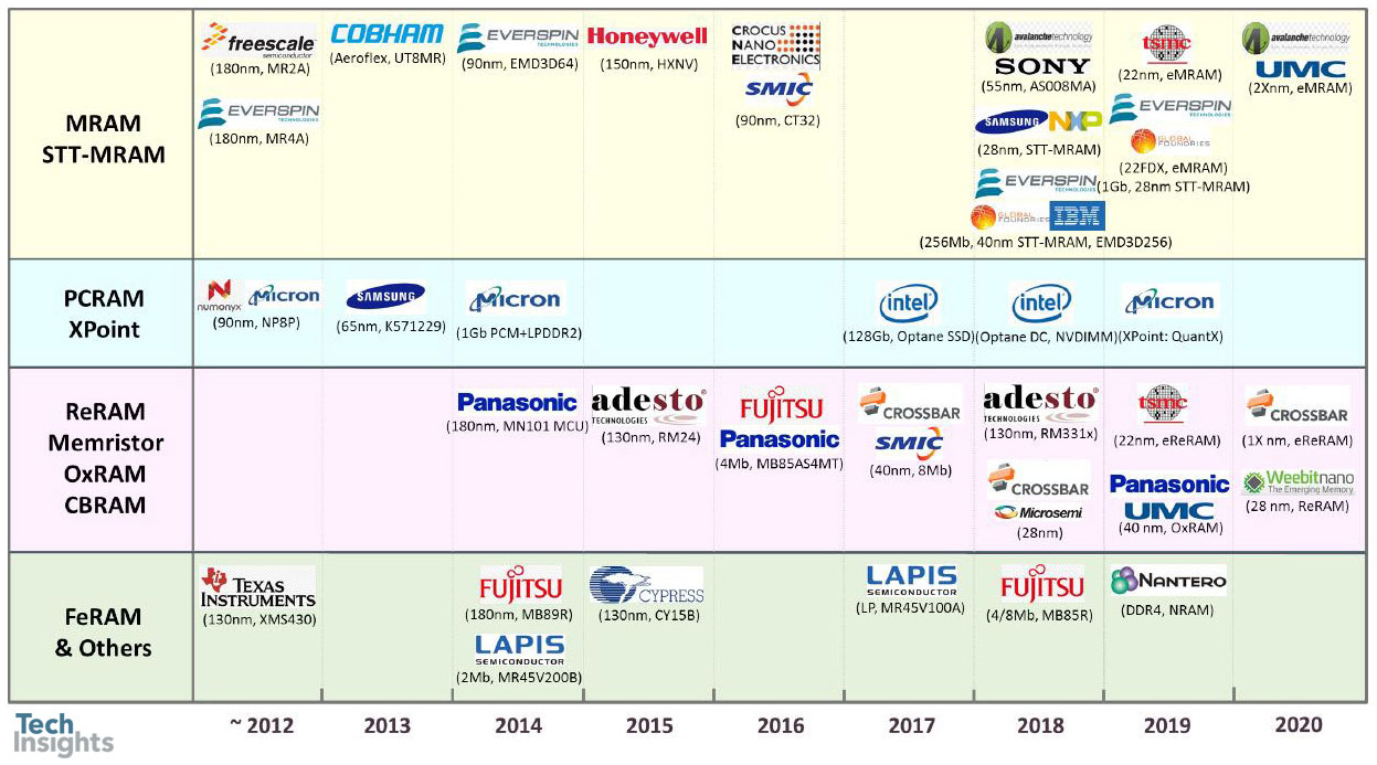
Jeongdong finished his talk with a review of emerging memories – though how “emerging” some of them are is up for debate, since some products have been around for a while now. Here’s the roadmap:
Adesto Technologies CBRAM Updates
For example. Everspin has been making MRAM of various sorts for a while now, phase change memory (PC-RAM) has been trialled on numerous occasions by a number of companies, and Fujitsu has been shipping its FeRAM for years.
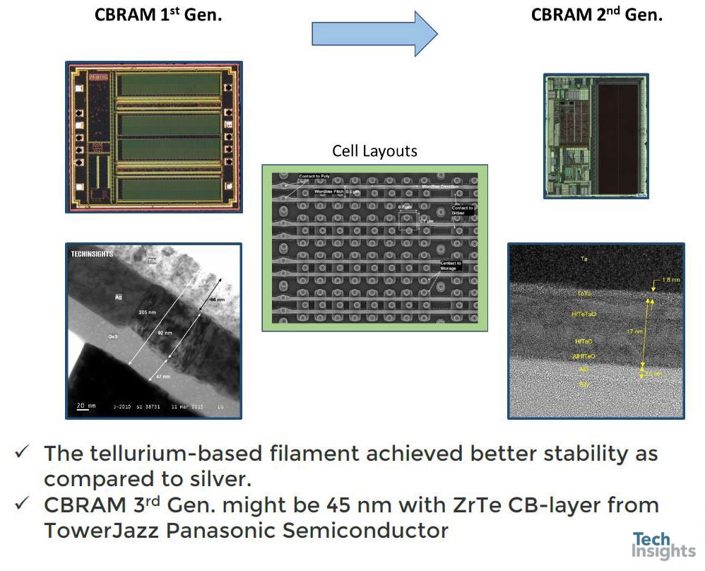
The first example was the Adesto CBRAM (conductive bridge RAM), detailing the change between their first- and second-generation CB memories.
Everspin SST-MRAM 2nd Gen.
Structurally, the bridge layers have changed from silver/germanium sulphide to a tellurium-based multi-layer stack, which I presume is less temperature-sensitive than the silver.
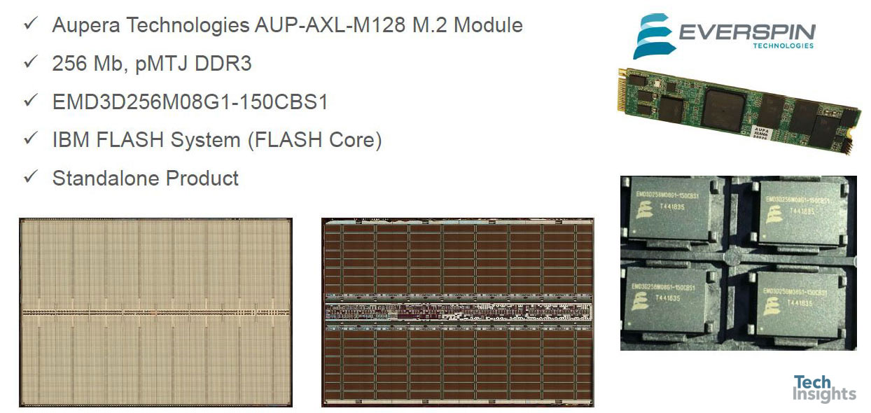
Then we were shown the 256-Mb Everspin 2nd-gen STT-MRAM, using perpendicular-MTJ (magnetic tunnel junction) technology in a DDR3 format.
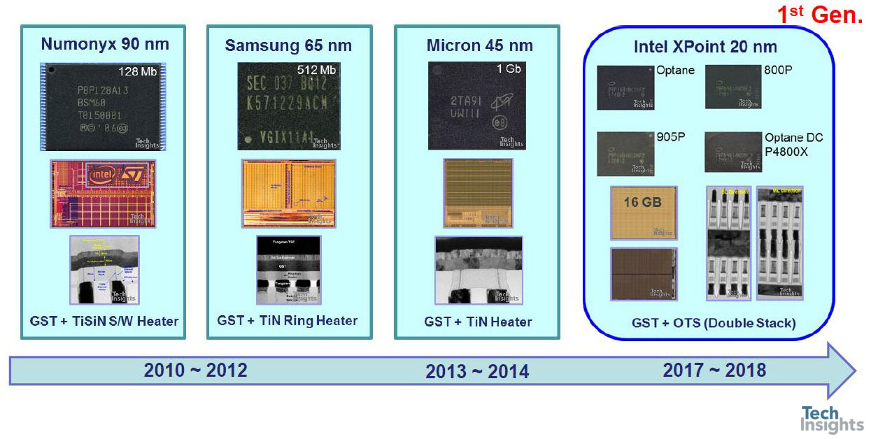
PCM Commercial Products: 2010 - 2018
As a lead-up to the 3D-Xpoint slides which completed the talk, we were reminded that PC memory has been around for a while, and we have gone from 128 Mb from a 90-nm process to 20-nm 16 Gb:
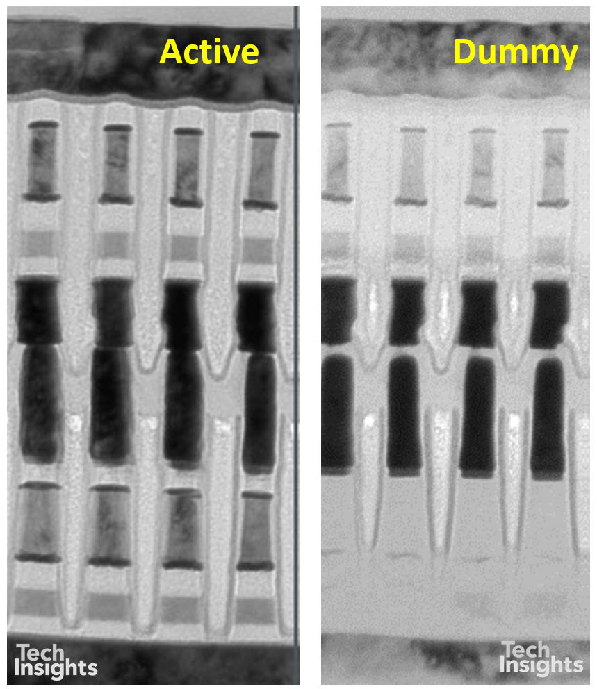
It appears that, at least in the Intel Optane version of 3D Xpoint, there are dummy memory blocks at the memory level (i.e. between metals 4 and 5), which have no drive circuitry, so that the circuit area is different from the memory array area. There are also structural differences in the double stack of the memory cells; in the lower cells it appears that the storage and selector layers are missing (though there are enough shadows of them in this image that the disappearance could be a sample-prep artefact). However, the tungsten wordlines in the centre are clearly separated.
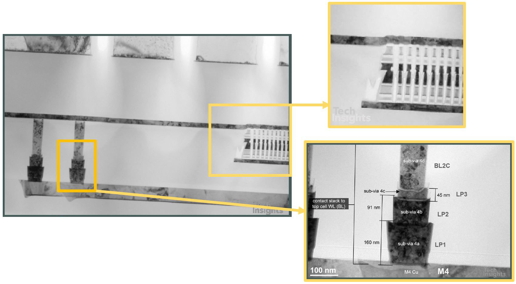
This stacking of the two layers of course adds to the process complexity, since we have to double up the deposition, etch, and photo steps; and in the bottom layer the wordlines are at the top of the stack, whereas the top stack has the wordlines at the base – and the reverse for the bitlines.
Adding the memory layers between M4 and M5 provides other challenges to the via structure between those layers, requiring more mask layers and the associated cost. The upper wordlines and bitlines are actually connected from below; as an example, the bitlines have a stack of four sub-vias to get up to the top bitline level.
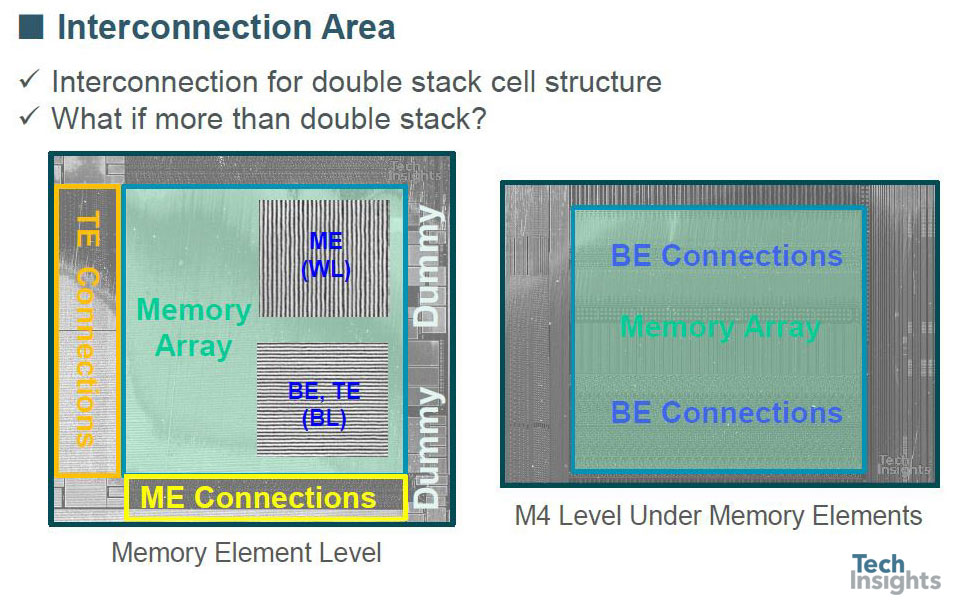
Insights & Issues: Process/Design Views
In plan-view it looks just as complex, so this poses the question – what do we do if we want to go to more than a double-stack structure? (BE/ME/TE = bottom/middle/top electrodes.)
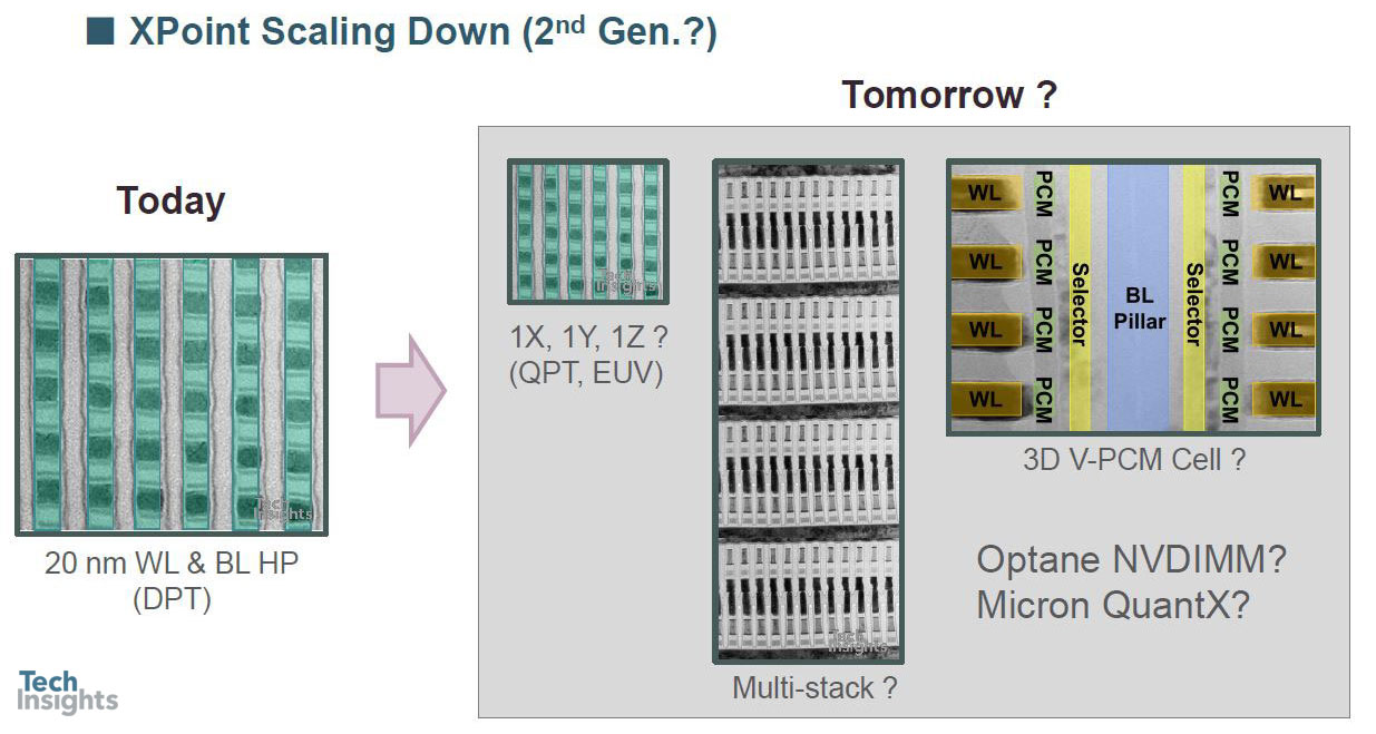
Insights & Issues: Process/Design Views
At the moment double patterning is being used, but of course there is the prospect of going to quadruple patterning, or even EUV, and maybe a multi-stack or 3D structure;
That concluded the talk, but don’t forget that all of this information, and a lot more, is available through the Memory Subscription from TechInsights.


