Posted: July 24, 2017
Contributing Authors: Ray Fontaine
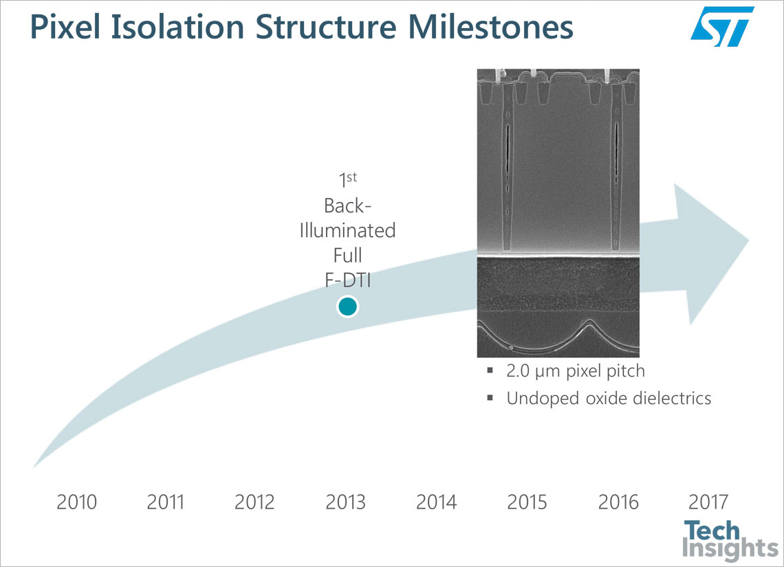
The third topic addressed in the IISW 2017 paper was an overview of the trends we’re seeing in pixel isolation structures. These structures are critical to the performance of 1.0 µm to 1.4 µm generation pixels in smartphone cameras. Going forward, we expect to see these structures deployed in other imaging applications, and for sub-micron pixels.
The full version of the TechInsights paper will be posted to the IISS website in August. As always, a thank-you is due to the IISW organizing committee for the opportunity to present and to our talented lab staff and analysts who generate the underlying data. Stay tuned – there is never a dull moment in the image sensors sector!
Pixel Isolation Structures
A wide range of structures have been fabricated on back-illuminated substrates to provide improved electrical and optical isolation. DTI process modules have been implemented both early in the process flow (prior to active device formation) and much later (after CIS back-of-die thinning). Most B-DTI structures in use to date have been filled with dielectrics, including a variety of high-k films.
The first DTI structures for back-illuminated CIS were found in 2010 in the HTC One UltraPixel camera chip fabricated by STMicroelectronics [25]. These early front-fabricated DTI (F-DTI) structures were built using silicon-on-insulator starting substrates. Current back-illuminated CIS chips are typically fabricated on back-thinned epi/bulk substrates.
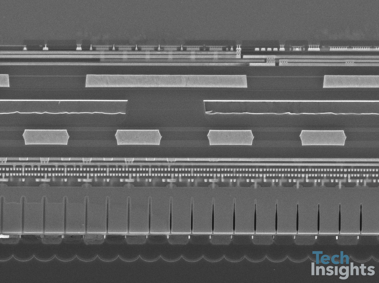
Fig. 3. Sony IMX260 – Exmor RS with DBI Technology Platform
A. Sony
Sony’s first observed DTI effort was a B-DTI structure found in the IMX147 in 2013 [26]. The B-DTI penetrated about 0.3 µm deep into a 2.8 µm thick substrate and was filled with a first interfacial oxide followed by HfO, TaO, oxide, a Ti-based liner and W metal. This chip is the only example of a metal filled trench from Sony. By 2015 Sony switched to a deeper, dielectric filled B-DTI structure comprising a thin interfacial oxide, AlO, TaO, and an undoped oxide core.
Fig. 3 shows a recent, dielectric-filled B-DTI structure from the 1.4 µm pixel generation IMX260 featuring a 2.9 µm thick substrate. The B-DTI extends to a nominal depth of 1.9 µm from the back surface, although it extends to a depth of 2.4 µm deep at B-DTI intersections.
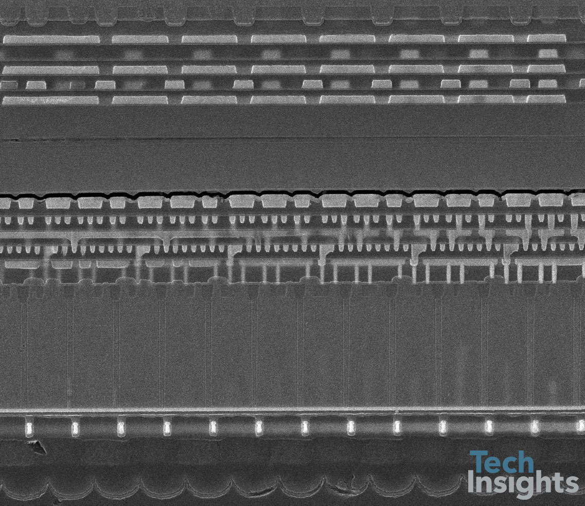
Fig. 4. Samsung S5K3P3SX Stacked ISOCELL Technology Platform
B. Samsung
B-DTI and F-DTI structures have been integrated to Samsung’s ISOCELL technology platform. Analyses to date indicate Samsung’s preference for full-depth F-DTI for 1.0 µm pixel generation ISOCELL and partial-depth B-DTI for 1.12 µm and 1.4 µm pixel generation ISOCELL structures.
The first observed B-DTI structures from Samsung, implemented in a 1.12 µm pixel generation chip in 2015, featured B-DTI trenches extending 1.3 µm deep into a 2.6 µm deep substrate.
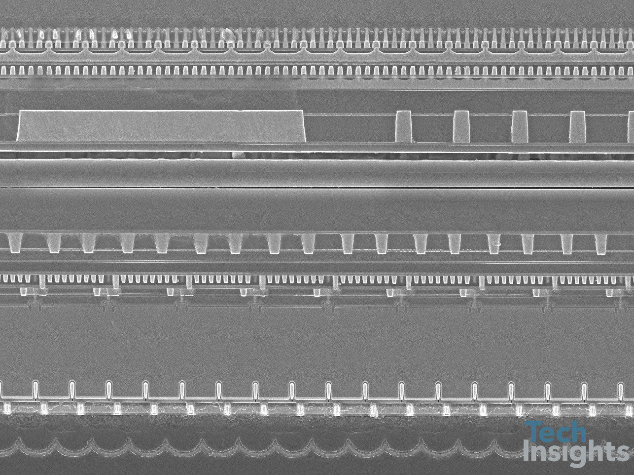
Fig. 5. OmniVision OV16880 PureCel Plus-S Technology Platform
C. OmniVision
OmniVision introduced partial B-DTI structures through its PureCel Plus-S technology platform, analyzed in 2016 [10]. The TSMC-fabricated structures for a 1.0 µm pixel generation CIS, extended 0.45 µm deep into the back surface of a 2.5 µm thick substrate. The B-DTI trench fill comprises an interfacial oxide, first deposited HfO, TaO, oxide, Ti-based liner, and a W core. To date, this is the only observed DTI structure on an OmniVision chip and the first metal filled B-DTI trench since Sony’s effort in 2013.
Get regular, succinct analysis of high-volume imaging and emerging applications
References
[1] FujiFilm press release, Jul. 21, 2010.
[2] “Fujifilm MS3961 Die Markings 12.0 MP, 1.6 μm Pixel Size CCD Image Sensor from Fujifilm FinePix Z800EXR Focused Technology Analysis (FTA) Report”, IPR-1009-801-01, -03, -04, -05, Oct. 2010.
[3] Nikon press release, Sep. 2011.
[4] “Aptina MT9J007C1HS 12 Megapixel (10.1 Megapixel Effective) CMOS Image Sensor with DR-Pix™ Technology from a Nikon V1 Camera Imager Process Review”, IPR-1110-804, Dec. 2011.
[5] Canon EOS 650D press release, Jun. 2012.
[6] “Canon LC1270 18.0 MP, 4.3 μm Pixel Size, APS-C Format CMOS Image Sensor from Canon EOS Rebel T4i (EOS 650D/EOS Kiss X6i)”, IPR-1206-802, Aug. 2012.
[7] “Sony IMX270, Micro Four Thirds, 20.4 MP Resolution, 3.3 µm Pixel Pitch, Front-Illuminated “Live MOS” CMOS Image Sensor from Olympus OM-D E-M1 Mark II MILC”, DEF-1703-802, Apr. 2017.
[8] Fujifilm press release, Jan. 2013.
[9] “Toshiba TCM5112CL CMOS Image Sensor from Fujifilm X20 Device Essentials Summary”, DEF-1311-803, Nov. 2013.
[10] “OmniVision OV16880, 1/3.06” Format, 16 MP Resolution, 1.0 μm Pixel Pitch Stacked (PureCel Plus-S) Back-Illuminated CMOS Image Sensor”, DEF-1606-804, Aug. 2016.
[11] Sony Xperia Z5 product page, Oct. 2015.
[12] Canon EOS 70D press release, Jul. 2013.
[13] Samsung press release, Mar. 2016.
[14] “Samsung S5K2L1, 1/2.6” Format, 12 MP Resolution, 1.4 μm Pixel Pitch Back-Illuminated Stacked ISOCELL CMOS Image Sensor from Samsung Galaxy S7 (Model SM-G930FD)”, DEF-1603-804, Apr. 2016.
[15] “Sony IMX260 12 MP, 1.4 μm Pixel Pitch Stacked BI CIS with DBI and Full Chip PDAF from the Samsung Galaxy S7 edge Rear-Facing Camera Imager Process Review”, IPR-1603-802, May 16, 2016.
[16] “Sony 12 MP Resolution, 1.0 μm Pixel Generation Stacked (Exmor RS) Back-Illuminated CMOS Image Sensor from iPhone 7 Plus Telephoto iSight Camera”, DEF-1612-801, Jan. 2017.
[17] Oppo R9s landing page, Oct. 2016.
[18] Kagawa, et. al, “Novel Stacked CMOS Image Sensor with Advanced Cu2C2 Hybrid Bonding” ISSCC2017. Feb. 2017.
[19] Invensas corporate web site, Apr. 2017.
[20] “Sony ISX014 1/4 Inch 8 MP, 1.12 μm Pixel Size Exmor RS Stacked Back Illuminated CIS Imager Process Review”, IPR-1302-801, Mar. 2013.
[21] “Sony IMX278 13.0 MP Exmor RS™ RGBW Stacked BI CMOS Image Sensor Extracted from the Huawei P8 Imager Process Review”, IPR-1505-801, Jul. 2015.
[22] “OmniVision OV23850 PureCel-S 1.12 μm Pixel, 23.8 MP Stacked CMOS Image Sensor from Gionee GN9008”, DEF-1508-802, Sep. 2015.
[23] “Samsung S5K3M2 13 MP Stacked, ISOCELL CMOS Image Sensor from Vivo X5Pro”, DEF-1507-801, Jul. 2015.
[24] P. Enquist, “Stacked image sensors - the new image sensor standard”, 2015 Image Sensors Europe, Mar. 2015.
[25] “STMicroelectronics 5 MP, 1.4 μm Pixel Pitch CMOS Image Sensor (5953BA Die Markings) Imager Process Review”, IPR-1003-802, Apr. 2010.
[26] “Sony IMX147 20 MP, 1.2 μm Pixel Pitch Back Illuminated (Exmor R) CMOS Image Sensor from the Sony Cyber-shot HX300 Digital Compact Camera”, IPR-1307-801, Sep. 2013.
[27] “Samsung S5K3P3SX 16 MP, 1.0 μm Pixel Pitch Stacked BSI Full ISOCELL CIS from the Samsung Galaxy A8 Smartphone Primary Camera Imager Process Review”, IPR-1509-801, Jan. 2016.


