Posted: May 2, 2017
Contributing Authors: Dick James, Fellow Emeritus
During the ISSCC conference last February, Sony issued a press release describing “Industry's First 3-Layer Stacked CMOS Image Sensor with DRAM for Smartphones”. There have been rumours of image sensors with embedded DRAM (to speed up the image data processing) for several years, but so far, nothing has been put into production and out in the real world.
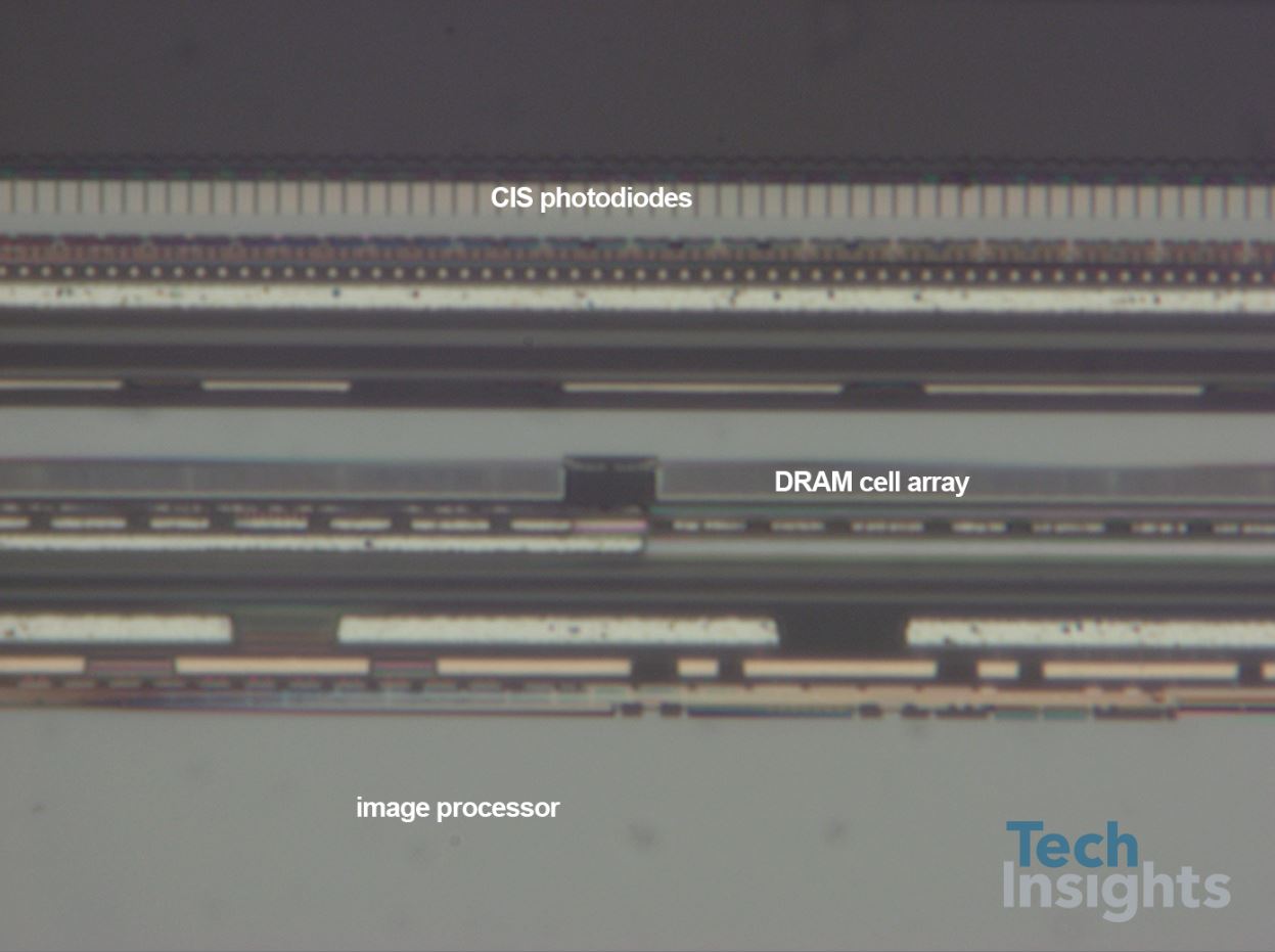
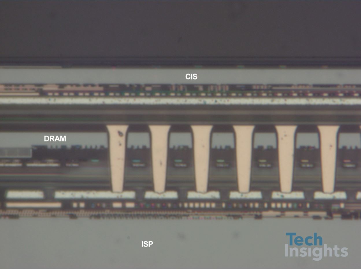
The details were given in a paper [1] at the ISSCC conference and it actually looked like the real thing, so this definitely caught the attention of our image-sensor experts inside TechInsights. Confirming its production status, at Mobile World Congress, Sony announced their Experia XZ Premium and XZs phones, with the Motion Eye™ camera system capable of 960 fps. We got hold of an Xperia XZs as soon as it was available, cross-sectioned the rear-facing camera chip, and lo and behold, we indeed have a three-stack; the CMOS image sensor (CIS) is mounted face-to-back on the DRAM, which is face-to-face with the image signal processor (ISP).
Download a Summary of our Analysis Offerings
This product brief summarizes the deliverables that we intend to build as well as some additional commentary on the technological relevance of the part.
However, we are getting ahead of ourselves a little, so let’s take a look at Sony’s press release and the ISSCC paper.
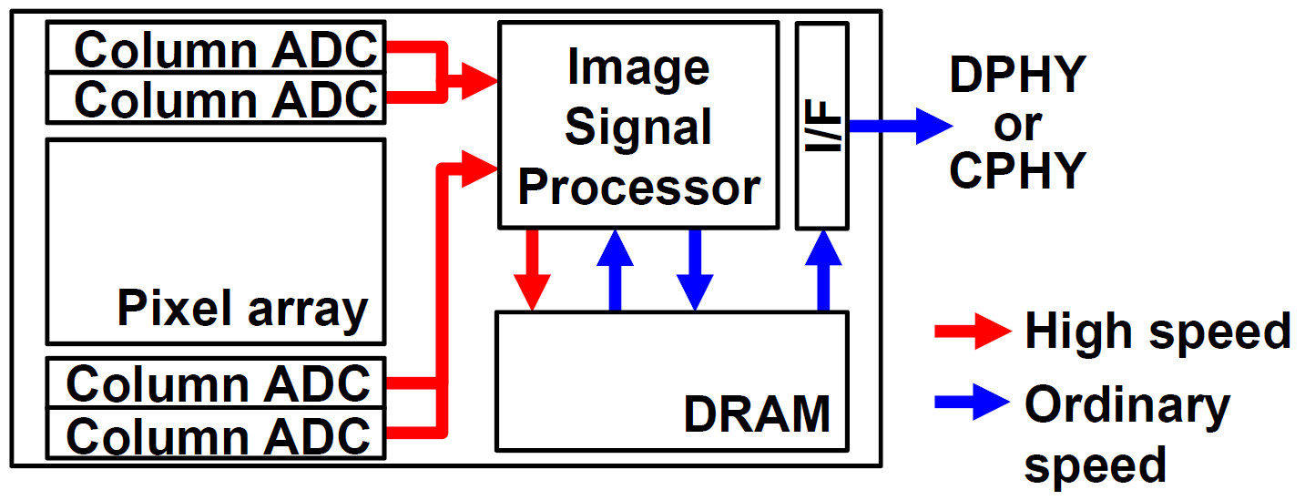
In its earlier 19 Mp image sensor, Sony used dual digital/analog converters to digitize the pixel data, and now we have a 4-tier construction to increase readout speed, and improve processing capability. The DRAM is used to temporarily store the high-speed data, and then output it at the optimal rate for the sensor interface. This design allows it to read a still image of 19.3 million pixels in only 1/120 of a second, and in movie mode it can go up to ~1000 fps, ~4x and ~8x (respectively) faster than the earlier product. This block diagram illustrates the signal path.
Given that the DRAM is sandwiched between the CIS and the ISP, the high-speed data has to go through the memory chip to the ISP, and then back-and-forth until it is output through the I/F (interface) block of the ISP, at a conventional speed suitable for the applications processor.
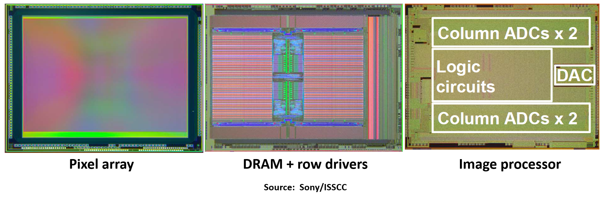
That’s a pretty compressed version of the sensor operation; the paper goes into more detail, including how the 960 fps imaging and slow-motion works. Sony’s schematic illustrates the three-stack.
According to the paper, the pixel array is in the top die, the DRAM array and row drivers are in the middle die, and the remaining blocks are in the bottom ISP die. We don’t have die photos of all three dies yet, but the paper had some images.
Sony also tells us that the CIS is made in a 90 nm, 1 Al, 5 Cu technology, the DRAM is a 1 Gb, 30 nm (3 Al, 1 W) part, and the ISP is a 40 nm, 1 Al, 6 Cu device. It was undoubtedly a challenge to get all the functionality required into three dies of the same size, without wasting silicon area.
Given that the DRAM die also has the CIS row drivers on it, then it must have been designed as a custom part, and is not one of the TSV-enabled (TSV = through-silicon via) commodity DRAMs that we have seen in recent years. Sony’s cross-section also shows that the center die has a thick back oxide and landing pad for TSVs coming down from the CIS above.
We can also see (if the scale bar is accurate), that the CIS and DRAM die substrates have been thinned down to ~2.6 µm, normal for a back-illuminated CIS (BI-CIS), but that’s the thinnest DRAM we have ever seen. Our own image (above) confirms that the CIS and DRAM silicon are of the same order in thickness, and the landing pads are also visible.
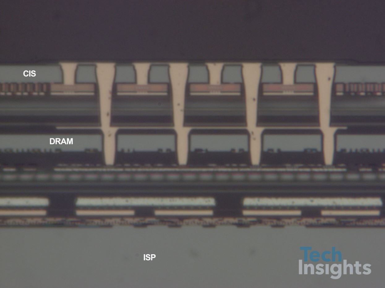
The next question is – how have the TSVs been formed in the stack? Our first cross-sections have just come out of the lab, and they look quite familiar. The CIS/DRAM connection seems to be the up-and-over form of TSV that we have seen in earlier generations of Sony back-illuminated (BI) CIS devices.
Here there are two layers of TSVs connecting what looks like a 6-metal stack in the CIS to the M1 of the DRAM die. We do not have a cross-section of extended TSVs joining the CIS directly to the ISP, though there are TSVs through the DRAM to the top metal of the ISP.
It seems likely that the CIS/ISP connection could use the DRAM landing pad layer as an interconnect, to avoid the challenge of drilling through two dies after the full stack was formed.
Further analysis of the IMX400 is ongoing, and in due time we will have reports on the CIS itself as well as the package stack. In industry terms, Sony has again pushed the limits of what can be done with mobile phone cameras. The big question for later this year is – will we see this in the next iPhone?
Reference:
[1] T. Haruta et al., “A 1/2.3-inch 20Mpixel 3-layer Stacked CMOS Image © 2017 IEEE Sensor with DRAM”, Proc. ISSCC 2017, paper 4.6


