SK hynix 321-Layer 4D NAND
What a single image can tell us

Share This Post
The recent Flash Memory Summit (FMS) 2023 provided several interesting updates —one is the SK hynix 321-L 4D NAND (3D NAND with peri under cell) prototype.
The FMS keynote revealed that SK hynix applied a “cost-effective three-plug integration” process. (Similar triple-plug processes are observed in Intel/Solidigm 144-L 3D NAND and 192-L 3D NAND). The memory cell film depositions were increased from single runs to triple runs. The reduced aspect ratio (AR) for each run allow better cell film uniformity, leading to better yield.
Figure 1 shows an annotated image of SK hynix 321-L 4D NAND (captured during FMS 2023). There is no noticeable change for the PUC scheme and the source plate. Table 1 shows a comparison between the SK hynix 176-L 4D NAND and 321-L 4D NAND.

Figure 1: SK hynix 321-L 4D NAND as presented at FMS 2023. Annotations by TechInsights, 2023.
| Features | Sk hynix 176-L AME-2206-801 |
Sk hynix 321-L Figure 1 |
|---|---|---|
| Scheme | Peri. Under Cell | Unchanged |
| Source Plate | Stacked | No Visible Change |
| WL Pitch | 45 nm | ~40 nm |
| Slit Pitch | 1.5 μm | Doubled |
| Deck | 2 | 3 |
| Inter-deck(s) | No Additional Layer | No Visible Change |
| Plug | 1 | 3 |
| WL Separations | Drain side only | Drain & Source Sides |
| Active VC Between Slits | 8 | Doubled |
Table 1: Comparison of SK hynix 176-L vs. 321-L. TechInsights, 2023.
Micron 232-L 3D NAND
The vertical channel (VC) tube/pillar configuration is similar to the Micron 232-L 3D NAND (Figure 2). Four sub-blocks are formed with the use of three wordline (WL) separations (drain side) between the slits.
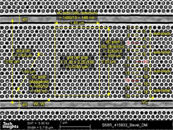
Figure 2: Top-down SEM image of Micron 232-L 3D NAND. TechInsights, 2023.
WL separation (source side) is not commonly observed for CTF-based 3D NAND; however, we observed this feature in the YMTC 232-L 3D NAND.
Figure 3 shows our analysis based on Figure 1 and an assumption that the WL pitch is 4x nm; we measured the slit depth and pitch, stacked VC height, and source plate thickness. The slit pitch and source plate thickness fall within expectation, which assists in the validity of the assumption. The total WL count is expected to be 345. (Note: Precise calibration is not possible as a physical sample was not available.)

Figure 3: Expectations of SK hynix 321-L 4D NAND. Annotations by TechInsights, 2023.
A possible configuration of the WLs is shown in Table 2.
| Deck (VC) | Function | # of Layers |
|---|---|---|
| D3 (VC3) | Selector | 5 |
| D3 (VC3) | Dummy WL | 2 |
| D3 (VC3) | Active WL | 101 |
| D3 (VC3) | Dummy WL | 2 |
| D2 (VC2) | Dummy WL | 2 |
| D2 (VC2) | Active WL | 110 |
| D2 (VC2) | Dummy WL | 2 |
| D1 (VC1) | Dummy WL | 2 |
| D1 (VC1) | Active WL | 110 |
| D1 (VC1) | Dummy WL | 2 |
| D0 (VC1) | Selector | 7 |
Table 2: Possible configuration of SK hynix 321-L WLs. TechInsights, 2023.
With the absence of (additional) inter-deck layers, the WL pads (staircase) scheme for the SK hynix 321-L 3D NAND can be handled in a similar manner to SK hynix 176-L 3D NAND. Details are available in the SK hynix 176-L 3D NAND process flow analysis.
We look forward to conducting further analysis when physical samples are available. Until then, it is best to take my preliminary analysis with a pinch of salt.


