An Ultra-Wide-Band Device Comparison
Like Bluetooth, the UWB is a short-range, low-power, radio-based communication technology whose primary purpose is for location discovery and device ranging. However, UWB offers a multitude of different functions, such as fast and reliable file-sharing features and secure transactions.

Jefferson Chua
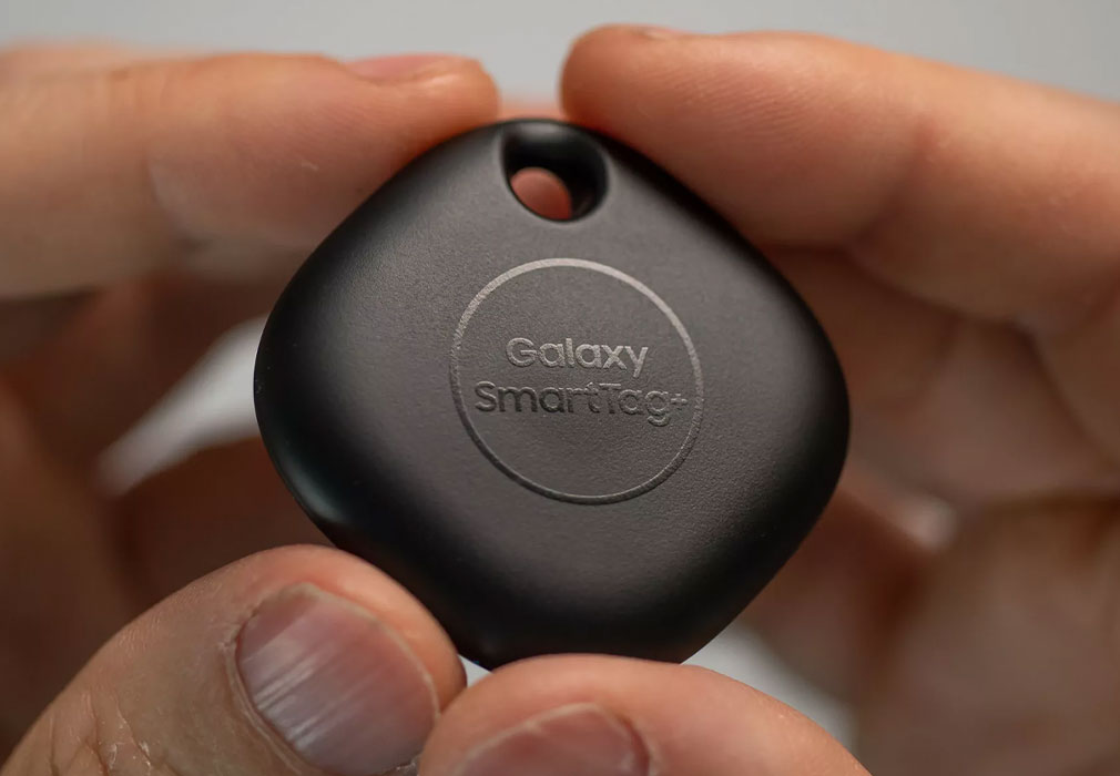
Samsung SmartTag+
On Thursday nights, I typically like to order a regular pepperoni pizza from my favorite place. However, a couple days ago, I made a blunder…
When the pizza delivery guy was outside my door a few days ago, of course this was the perfect time for me to lose my wallet. I raked through my memory, attempting to remember where I put the thing. At this point, I almost admitted defeat, thinking I’d have to go through the humiliation of telling the pizza delivery guy I couldn’t pay for my pizza.
Luckily, my smart phone was able to track its whereabouts via a planted tracker. This tracker uses Ultra-Wide Band (UWB) technology.
Subscribe to TechInsights Blogs
Join our list to get the latest blog posts directly in your email.
This blog, we have the pleasure of looking at the NXP SR040 UWB transceiver-processor die that was extracted from the Samsung EI-T7300 (SmartTag+).
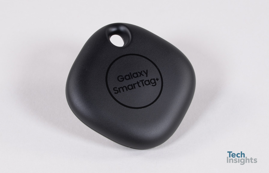
Figure 1. Samsung EI-T7300 (SmartTag+)
The NXP Semiconductor SR040 is housed in a QFN package which comprises of a single die that is wire bonded to the lead frame. These measured critical dimensions, along with the observed features of the transistors, suggest that the SR040 die is using TSMC’s 40 nm CMOS process.
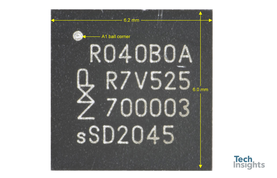
Figure 2. NXP Semiconductor SR040
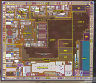
The SR040 die consists of a UWB analog-front end transceiver, several power management circuitries, several SRAM memories, an ARM Cortex CPU, and several GPIOs.
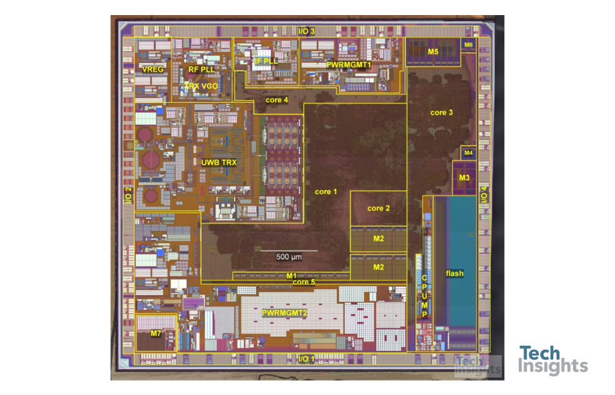
Figure 3. NXP Semiconductor SR040 die photo
Let us a take at the UWB analog-front-end transceiver more closely.
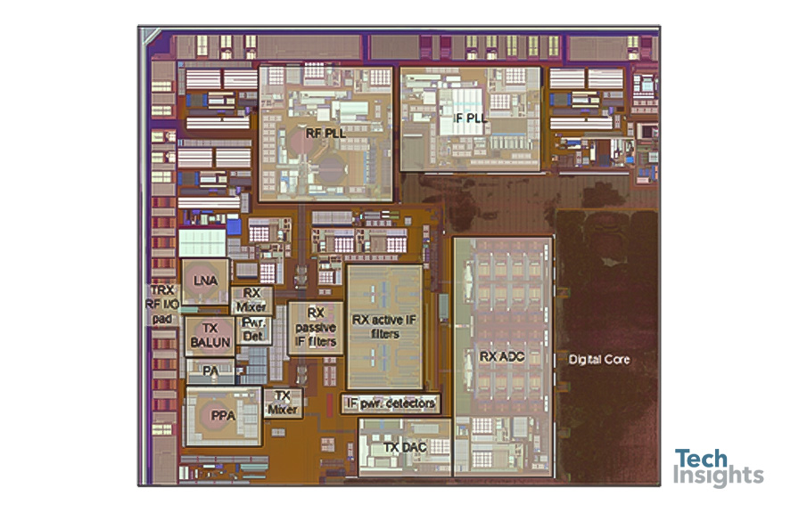
Figure 4. UWB analog-front-end transceiver
The UWB transceiver macro can be divided into two halves. In the bottom half, we find the RF signal path while the RF and IF PLL are in the top half. A single RF bonding pad is shared between the receiver and transmitter.
The receive path includes the LNA with its input matching circuit, the RX quadrature down-converter mixer, a pair of passive filters, a pair of active filters consisting of two second order stages, and lastly, a pair of time-interleaved ADC with each including successive approximation sub-ADCs.
The transmit line-up consists of the TX DAC consisting of two, cascaded sub-DACs, the upconverting TX mixer, the power amplifier, and the BALUN transformer.
The RF PLL includes identical L-C tank-based oscillators. The quadrature phases required by the receiver are generated near the oscillator and sent to their destination using differential coplanar transmission lines. The transmitter uses one of the same two phases. Since the IF section of the transmitter is not quadrature, therefore the phase modulation must be generated in the RF PLL and impressed on the signal in the mixer. The clocks for the RX ADC and the TX DAC are generated in the IF PLL that includes a three-stage, differential CMOS ring oscillator.
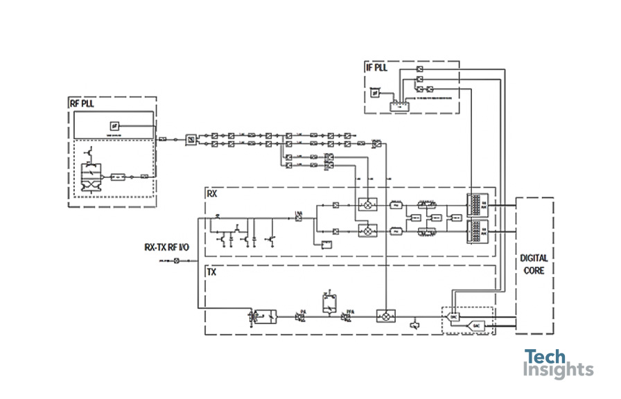
Figure 5. Circuit analysis
Now let us do a quick functional comparison between the NXP SR040 UWB vs. the Apple U1 (TMKA75 Die) UWB, which was taken from the Apple AirTag.
 |
 |
|
|---|---|---|
| Die Manufacturer / Device | NXP SR040 | Apple U1 (TMKA75) |
| Die Size (Seal) | 3.09 x 3.33 (10.29 mm2) | 2.97 x 3.27 (9.71 mm2) |
| UWB Transceiver and PLL (mm2 - % of the die) |
1.8 mm2 - 18% | 2.8 mm2 - 29% |
| Power Management (mm2 - % of the die) |
2.7 mm2 - 27% | 0.4 mm2 - 4% |
| Power Cores and their embedded memories (mm2 - % of the die) |
3.6 mm2 - 37% | 5.5 mm2 - 57% |
| Foundry and Process Generation | TSMC, 40 nm CMOS | TSMC, 16 nm FinFET |
| Number of Metal Layers | 8 (7 Cu, 1 Al) | 13 (12 Cu, 1 Al) |
Aside from the fact that both devices have similar die sizes and having TSMC as its foundry, they are very different. For instance, SR040’s UWB transceiver and power management occupies 45% of the die and only 33% for the Apple U1. In terms of the processor and memory area, it occupies 37% of the die for the SR040 and 57% for the Apple U1. The SR040 has a process generation of 40 nm and was formed using 8 metal layers while the Apple U1 has a process generation of 16 nm and was formed using 13 metal layers.
That concludes the brief summary of two devices employing UWB communication standard used for tracking objects.
Today, we are still in the early stages of UWB-based technology development, and concerns such as data privacy and efficiency will need to be improved, today, we know that UWB is used for replacing car keys or finding my wallet but in the future it could pretty much interface and track important objects with our “smarter” gadgets. Rest assured, Techinsights will always be monitoring these new devices.
Ensure you’re armed with the latest technical intelligence.
Sign up for a free trial today to see how the TechInsights Platform will help you.
Sample reports from this blog may be available with your free trial.


