Samsung D1z LPDDR5 DRAM with EUV Lithography (EUVL)
Finally! After months of waiting, we have seen Samsung Electronics’ applied extreme ultraviolet (EUV) lithography technology for D1z DRAM in mass production! Early last year, Samsung Electronics announced the world’s first development of both ArF-i based D1z DRAM and separately its EUV lithography (EUVL) applied D1z DRAM. TechInsights is excited that we have finally found Samsung’s new and advanced D1z DRAM devices and confirmed details of this technology.
Samsung Electronics has developed its D1z 8GB DDR4, D1z 12GB LPDDR5, and 16GB LPDDR5 DRAM devices as well with higher performance. We found both of the latter two devices (the D1z 12GB and D1z 16GB LPDDR5 chips) in the Samsung Galaxy S21 5G series; S21 5G, S21+ 5G and S21 Ultra 5G just released in January 2021.
12 GG LPDDR5 chips are being used for Samsung Galaxy S21 Ultra 5G SM-G998B/DS 12GB RAM, while 16 Gb LPDDR5 chips can be found in S21 5G and S21+ 5G 8 GB RAM components.
When it comes to the D1z technology node, Samsung’s D1z 12 GB LPDDR5 DRAM generation has more than 15-percent higher manufacturing productivity compared to the previous D1y 12 GB version. The design rule (D/R) is decreased from the 17.1 nm (in the prior D1y generation) down to 15.7 nm (D1z). The die size is also reduced, from 53.53 mm2 (D1y) to 43.98 mm2 (D1z); the die of the new chip is about 18% scaled down from the previous version (Table 1).
| Items | Samsung LPDDR5 Chips | |||
|---|---|---|---|---|
| Memory Capacity | 8 Gb | 12 Gb | 12 Gb | 16 Gb |
| Tech Node | D1y | D1y | D1z | D1z |
| Parent Product Example | Xiaomi Mi 10 | Xiaomi Mi 10 | Samsung Galaxy S21 Ultra 5G |
Samsung Galaxy S21/S21+ 5G |
| DRAM Component Example | K3LK3K30EM-BGCN | K3LK4K40BM-BGCN | K3LK4K40CM-BGCP | K3LK7K70BM-BGCP |
| Die Size | 39.12 mm2 | 53.53 mm2 | 43.98 mm2 | 61.20 mm2 |
| Bit Densoty (Die) | 0.205 Gb/mm2 | 0.224 Gb/mm2 | 0.273 Gb/mm2 | 0.261 Gb/mm2 |
| Cell Size | 0.00231 µm2 | 0.00231 µm2 | 0.00197 µm2 | 0.00197 µm2 |
| D/R | 17.1 nm | 17.1 nm | 15.7 nm | 15.7 nm |
| EUV Lithography Applied | No | No | Yes (BLP) | No |
A comparison of Samsung D1y and D1z LPDDR5 Chips with 8 GB, 12 GB and 16 GB.
Samsung Electronics used its most advanced D1z technology together with EUV lithography on 12 GB die with K4L2E165YC die markings, while D1z 16 GB LPDDR5 DRAM chips with K4L6E165YB die markings show non-EUV lithography die. It is likely Samsung initially developed D1z LPDDR5 products both with ArF-i based and EUV-based storage node landing pad / bit line pad (SNLP/ BLP) lithography, and now it produces all D1z LPDDR5 products with EUV SNLP/BLP lithography.
It applied HVM (high volume manufacturing) product in the DRAM industry and worldwide market, although Samsung released 1M sample modules with D1x EUV lithography applied in late 2019. Samsung D1z chips are likely fabbed from the second production line in Pyeongtaek, Korea.
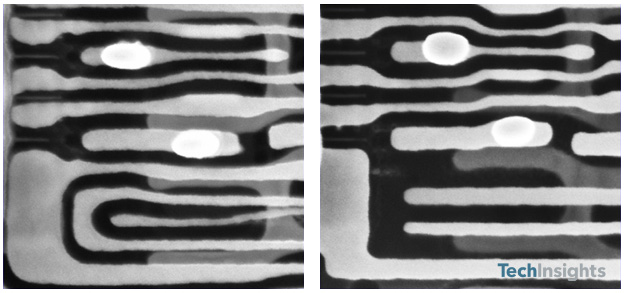
Samsung DRAM cell design, a comparison of BLP patterns on D1z (a) without EUVL and (b) with EUVL.
For DRAM process integration for D1z 12 Gb LPDDR5 devices, Samsung adopted EUV lithography technology limited to only one mask, a Storage Node Landing Pad (SNLP on call array)/Bit Line Pad (BLP on S/A) which measures around 40 nm critical dimension (CD or pitch) and 13.5 nm BLP line width on S/A (sense amplifier circuitry) area. Figure 1 shows a comparison of S/A BLP patterns on Samsung’s (a) D1z 16 GB LPDDR5 die with ArF-i based lithography and (b) D1z 12 Gb LPDDR5 die with EUV lithography. By using EUV lithography, BLP line edge roughness (LER) on S/A area is improved and bridge/short defects might be reduced.
| Device | Micron D1z | Samsung D1z | Samsung D1z |
|---|---|---|---|
| Memory Capacity | 16 Gb | 12 Gb | 16 Gb |
| Tech Node | D1z | D1z | D1z |
| Parent Product Example | MT53E1G32D2NP-046_WT:A (LPDDR4) | K3LK4K40CM-BGCP (LPDDR5) | K3LK7K70BM-BGCP (LPDDR5) |
| Die Size | 68.34 mm2 | 43.98 mm2 | 61.20 mm2 |
| Bit Densoty (Die) | 0.234 Gb/mm2 | 0.273 Gb/mm2 | 0.261 Gb/mm2 |
| Cell Size | 0.00204 µm2 | 0.00197 µm2 | 0.00197 µm2 |
| D/R | 15.9 nm | 15.7 nm | 15.7 nm |
| EUV Lithography Applied | No | Yes (BLP) | No |
A comparison of D1z DRAM; Micron D1z LPDDR4 vs. Samsung D1z LPDDR5 chips.
Compared to Micron Technology’s competing D1z cell design, Samsung further reduced cell size (Samsung is at 0.00197 µm2 versus Micron at 0.00204 µm2) and D/R (Samsung 15.7 nm vs. Micron 15.9 nm). Micron used ArF-i based lithography for all the photomask steps on D1z products, and it will not adopt EUV lithography for a while, including D1α and D1β. (Table 2)
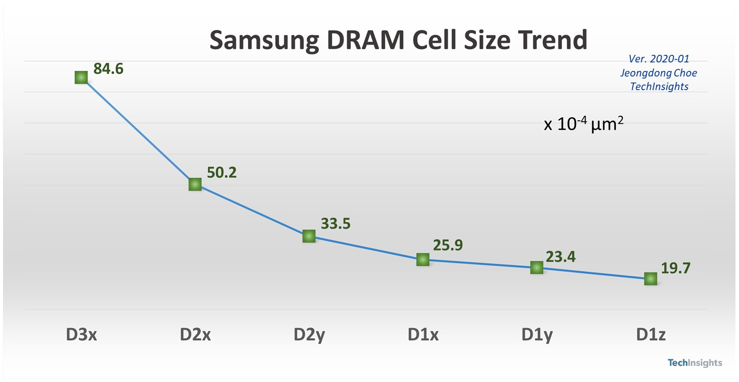
Samsung DRAM cell size trend, D3x through D1z
Samsung DRAM cell size and D/R trends are shown in Figure 2 and Figure 3, respectively, including D3x through D1z. DRAM cell size and D/R scaling are getting harder and harder recently, however Samsung reduced D/R to 15.7 nm for D1z, which is 8.2 % scaling down from D1y.

Samsung DRAM cell D/R trend, D3x through D1z
Samsung will continue to increase EUVL steps for the next DRAM generation such as D1a (in 2021) and D1b (in 2022).
Dr. Jeongdong Choe, Senior Technical Fellow
Dr. Jeongdong Choe is a Senior Technical Fellow at TechInsights. He has nearly 30 years of experience in the semiconductor industry, R&D and reverse engineering on DRAM, NAND/NOR FLASH, SRAM/Logic and emerging memory. He worked for SK Hynix and Samsung Electronics for over 20 years. He joined TechInsights and has been focusing on technology analysis on semiconductor process, device and architecture. He has written many articles on memory technology including DRAM technology trend, 2D and 3D NAND process/device integration details, and Emerging memory such as STT-MRAM, XPoint, ReRAM and FeRAM design and architecture. He quarterly produces and updates a widely distributed memory roadmaps on DRAM, NAND and Emerging memory.
Want to read more?
TechInsights Memory subscribers already have access to exclusive TechStream content in the TechInsights Platform.
Interested in a subscription?
TechInsights offers subscriptions to the broadest range of analysis and expert commentary. Contact us to learn about our many subscription offerings.


