ROHM Gen 4: A Technical Review
A collaboration between Dr. Stephen Russell (TechInsights) and Prof. Peter Gammon (PGC)

Dr. Stephen Russell

Prof. Peter Gammon
ROHM released their 4th generation (Gen 4) MOSFET products this year. The new range includes MOSFETs rated to 750 V (increased from 650V) and 1200 V, with a number of the available TO247 packaged components automotive qualified up to 56A/24mΩ. This is a line-up that suggests ROHM will continue to target the on-board charger market where they have had previous success.
In their release statement, ROHM claimed that their Gen 4 products “reduce ON resistance per unit area by 40% over conventional products without sacrificing short-circuit withstand time by further improving an original double trench structure.” They continue: “In addition, significantly reducing the parasitic capacitance makes it possible to achieve 50% lower switching loss over our previous generation of SiC MOSFETs”.
Within a few weeks, TechInsights quickly sourced and cross-sectioned the new ROHM 4th generation MOSFETs, releasing the first images in July 2022. Since then, PGC has been working to provide electrical data on these devices, which combined with the cross-sections help us interpret the advances ROHM have made in their trench technology.
In time, a full analysis, testing the device's robustness, reliability and beyond-the-datasheet characteristics will be made available for TechInsights subscribers. In the meantime, in this article, we shall make public some of our revealing early analysis that helps us validate the claim above made by ROHM, and understand the improvements they have made.
Trench MOSFET Basics
Conventional ‘planar’ MOSFETs have their gate and channel region located on the semiconductor surface. Planar MOSFETs are easy to manufacture and fairly reliable. However, in the drive to reduce chip size, and hence to drive up yields, its lateral topology imposes a limit as to how far, ultimately, it can be shrunk.
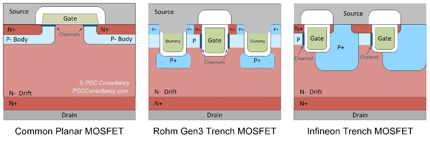
Figure 1: Representations of SiC MOSFET designs, showing the typical planar structure and trench designs form ROHM (Gen 3) and Infineon.
A trench MOSFET comprises a gate formed on the edge of a trench, that has been etched into the SiC surface. The trench gate is used to create a lower resistance device – a lower specific on-resistance (Ronsp, resistance x area) to be precise. Achieving a lower Ronsp allows the chip manufacturer to shrink down the size of the die, thereby achieving their RDSon=15 mOhm product, say, utilising less SiC, thus benefitting yields.
Multiple reasons lie behind the trench MOSFET’s lower Ronsp. First, a gate fabricated on a SiC trench sidewall has a higher channel mobility, meaning electrons are impeded less passing down through a trench gate than compared to the planar device. This reduces the channel resistance. Second, trench MOSFETs can possibly eliminate a planar MOSFET’s JFET resistance, the region in which the current from two channels are squeezed into a narrow passage between the p-body contacts. However, as we will see, practical, pragmatic design may lead to a JFET-like region being reintroduced. Third, a greater density of vertical trench gates should be possible compared to the number of planar gates, so decreasing cell pitch and increasing current density.
However, beware the sharks. Trench MOSFETs can be tricky to optimise for reliable, robust operation. In particular, successful designs must navigate the problem of maximising SiC’s high electric field (9x greater than Si’s) at the top of the device, while protecting the delicate gate oxide, which is also located at the top of the device from the same field. This balancing act requires clever but intricate device layouts, or else the drift region will require serious derating, eroding the gains of the trench architecture. A disadvantage of trench MOSFETs is therefore their more complicated design, typically requiring a greater number of fabrication steps, a few of which may have particular complication– deep high energy implants (in the case of Infineon’s), or deep trench etches (ROHM Gen4’s).
ROHM and Infineon’s trench designs
ROHM and Infineon were the first to shift to trench MOSFETs, utilising very different designs. TechInsights cross section of ROHM’s Gen 3 is shown in Figure 2 below, as well as the cartoon form in Figure 1. ROHM opted for a more traditional design with channels down each side of every gate trench, utilising dummy trenches on each side, into which, deep P-implants protect the gate trench. Infineon made every trench work harder! Each trench has a channel down one side, the other side shrouded by a deep P+ implant that keeps the high electric field from the gate oxide. This layout allows the channel side of the trench to be perfectly aligned with the 4° off-axis SiC crystal; a neat trick that lowers its resistance.
Notable from Figure 3 are the two inactive source trenches between each active gate trench, and the wide body contacts, all of which make this a wide cell pitch for a trench device. However, when this device is seen in plan view, this apparently wasteful layout makes sense. Instead of traditional gate stripes spanning the device in only one dimension, this Gen 3 device is laid out with gates running both top-to-bottom and left-to right, creating a clever 2 dimensional grid of gates that nearly doubles the gate density per unit area. This was similar in its concept to Wolfspeed’s hexagonal layout that multiplies their gate density by around 1.3x.
Yet, until ROHM’s latest 4th Gen release, neither trench device could boast a Ronsp that was lower than the best-in-class planar MOSFETs. A further question for this Gen 3 design was just how much protection do the source trenches offer the gate from the very high fields present?
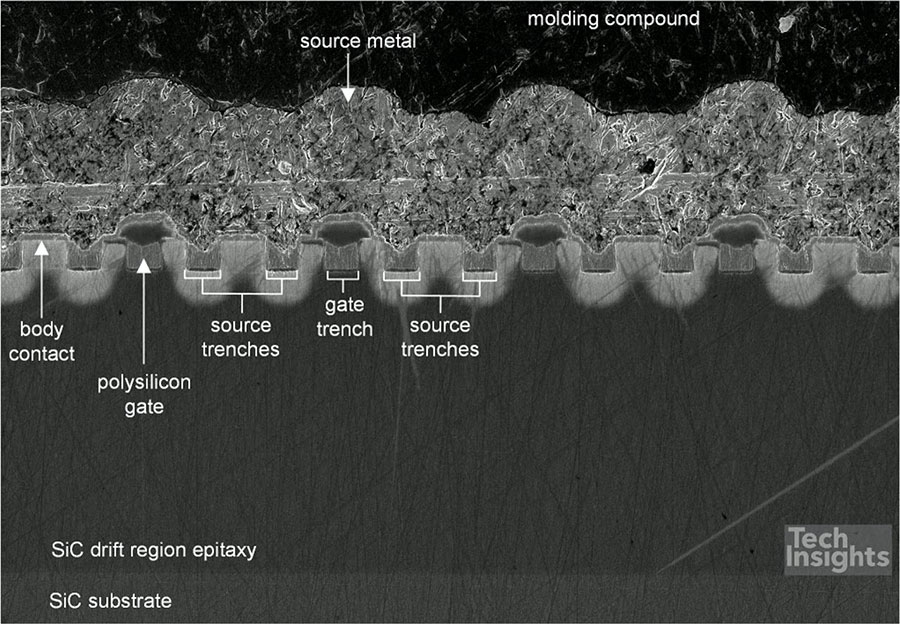
Figure 2: ROHM’s previous, 3rd Generation SiC MOSFETs (source: TechInsights)
ROHM’s 4th Generation SiC MOSFETs
After TechInsights quickly sourced and cross-sectioned the new ROHM 4th generation MOSFETs shown below is TechInsights high resolution SEM image of the new Gen 4 device.
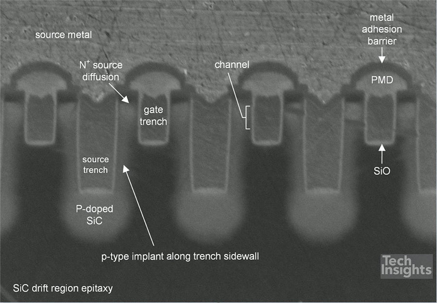
Figure 3: ROHM’s new, 4th Generation SiC MOSFETs (source: TechInsights)
When compared to the 3rd Gen device, the 4th Gen device has some similarities, and a number of striking differences.
What remains similar is the approach adopted by ROHM to use a traditional trench MOSFET design, with channels on both of the gate-trench sidewalls. Now, however, each gate trench is flanked by a single grounded source trench either side of it, that extends twice the depth into the drift region. As we shall explain, this is the key design feature, cleverly exploited by ROHM to better protect the gate oxide, and lower resistance.
The single dummy/source trench per gate trench allows a 3x reduction in cell pitch. However, this signifies the end to ROHM’s novel cell layout used in Gen 3, that nearly doubled the gate density, in favour of the traditional one-dimensional stripe layout. Taken together, this represents a net 50% (minimum) increase in gate trench density per unit area, which helps further drive down the problematic channel resistance that plagues other devices, a resistance that we have previously shown can contribute up to 30% of a 650V planar MOSFET’s series resistance.
Another major contributor to resistance, the substrate, has undergone thinning for the first time, vastly reducing this component.

Examining ROHM’s claims for their Gen 4 device
Using PGC’s extensive state-of-the-art electrical characterisation equipment, combined with the analysis from Techinsights, a number of ROHM’s claims for these devices have been examined. We compared directly, a new 650V 4th Gen Rohm MOSFET, a 3rd Gen MOSFET, and a best-in-class planar SiC MOSFET, all with similar Rdson ratings.
First to the losses. ROHM’s first claim in the image shown was that they had reduced their conduction losses by 40% allowing the equivalent chip size reduction. Indeed, with TechInsights cross sections, we can confirm that the specific on resistance (Ron × A) of the chip’s active area is almost exactly 40% lower than their previous generation, though in reality the necessary inactive areas of the device reduce this gain marginally. For further context, the new Ronsp is also 20% smaller than the leading planar device we have characterised. This is a crucial advance that allows the shrinking of die, forcing up yields driving down costs, as we have discussed previously.
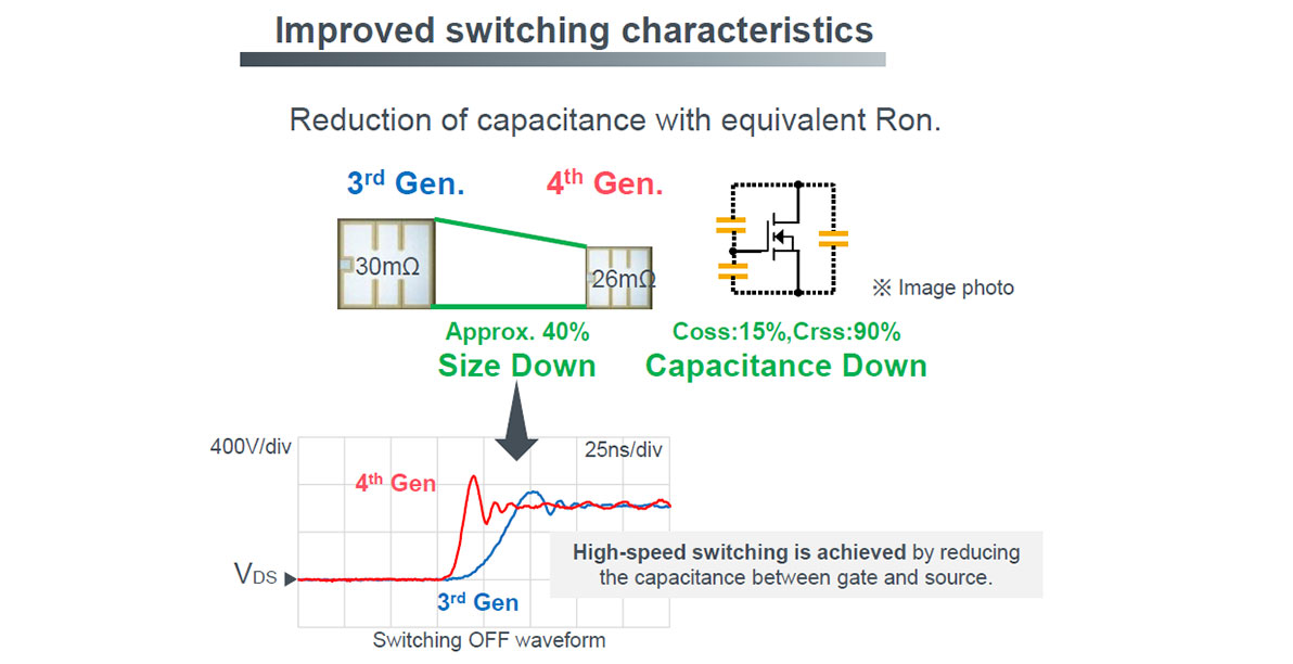
Figure 4: ROHM’s Gen 4s have lower Ronsp and reduced Coss and Crss (source: ROHM)
The second claim in the image is that the switching losses will be reduced due to the decrease in each of the miller capacitances. Indeed, while the die we were comparing were not perfectly matched, we could confirm a ~90% reduction in Crss (at rated voltage), and a fractional reduction in Coss, depending on voltage. Our own switching benchmarking tests are underway.
One claim made by ROHM relates to the increase in voltage rating of the range from 650 to 750 V. From ROHM: “750V breakdown voltage ensures design margin against VDS surge”. We find this an interesting development, one that is happening across the industry. In reality, however, the actual breakdown voltage of the new Gen 4 device, tested under static conditions, is ~1000V, which is actually lower than the Gen 3, which breaks down at over 1200V. The new Gen 4 is on a par with the leading planar device. To their claim about margin, well its quite impressive really, considering the actual data. They are signing off on their devices being used at 75% of their real breakdown voltage, up from just above 50% in Gen 3, a sign that they are considerably more reliable. This reduction in derating is a great improvement, one that in part, enables the resistance reduction, as we will explain in the next section.
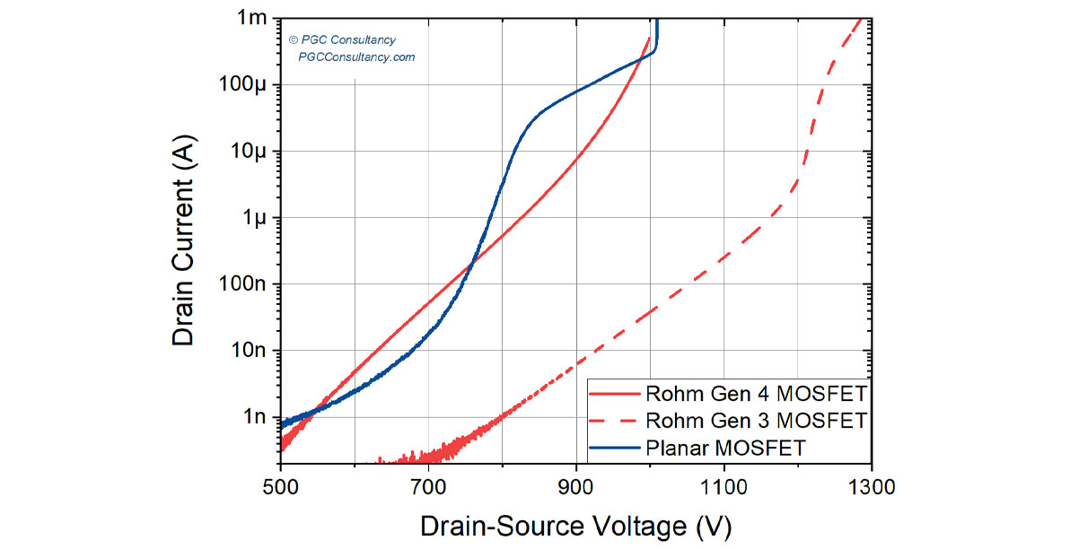
Figure 5: The true, measured breakdown voltage shows a reduction from Gen 3 to Gen 4, despite the increase in rated voltage. This represents a significant reduction in drift region derating.
Short circuit testing the Gen 4’s in the PGC labs will follow soon, but a third interesting claim of ROHM’s is that despite shrinking the die size and increasing the current density, their short circuit withstand time has actually increased. Taken at their word, this is further evidence combined with the derating reduction, that ROHM have taken a big step forward in the reliability and robustness of their devices.
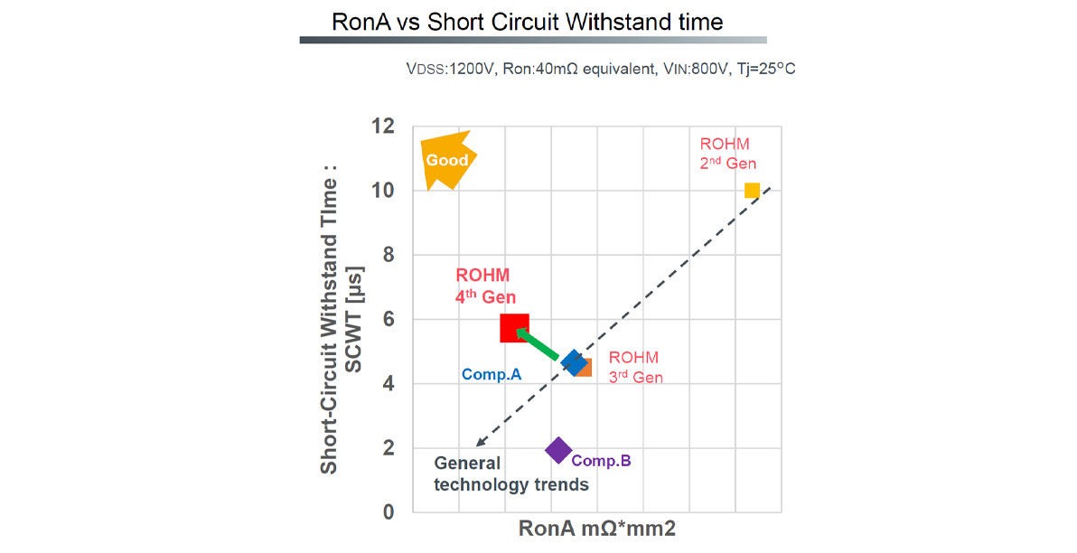
Figure 6: Rohm’s Gen 4s are said to increase short circuit withstand time, while simultaneously lowering Ronsp (source: ROHM)
Put together, this is a strong showing from ROHM, one that answers many of the criticisms of early SiC trench devices. Yet how has all of this been possible?
Rule 101: Protect the gate oxide
Pictured in the Figure below is PGC’s diagrammatic replication of the new Gen 4 design. This doesn’t consider the pitch reduction, rather it emphasises the changes around the gate.
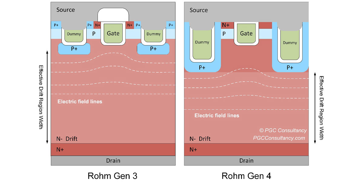
Figure 7: PGC’s representation of the new Gen 4 ROHM devices, complete with electric field lines, demonstrating how the gate oxide is protected.
So much about MOSFET design, particularly SiC trench MOSFET design, is about protecting the gate oxide when the device is in the off-state, blocking a large voltage. At this point, high electric fields are present at the device surface, which if allowed to coincide with the gate oxide cause problems with gate leakage and reliability. In the Gen 3 device, the source trenches were only as deep as the gate trench, and therefore, the P+ implants beneath these were only a little deeper than the gate trench itself. As a result, the electric field lines pictured in the diagram (which can be imagined as the outer edge of a balloon being inflated), bend around the trench corners, and can more easily interact with the bottom of the gate trench.
Conversely, ROHM’s new Gen 4 source trenches, which are surrounded by P+ regions implanted into the source trench sidewalls and bottom, are much deeper. This pushes the p-n junction that protects the gate down deeper into the drift region, further away from the gate oxide it is protecting. As shown in the Gen 4 diagram, the peak field line (the outer edge of the balloon) remains far from the gate oxide.
Gate Protection, the payoff
The gate is better protected, so what? Well, if the gate is relatively unprotected, as in the Gen 3 device, then action needs to be taken to ensure that the electric field never reaches a value high enough to cause damage. Therefore, the drift region that supports the blocking voltage is overdesigned (essentially derated - see my article on that subject) to support a larger than necessary voltage for the application. Recall that the 650V Gen 3 device, which could be used in 400V EVs, had a breakdown voltage of over 1200V. While this ensures safe long lasting operation, the penalty paid is that the resistance of the drift region rises exponentially with the voltage it can support (Rdr ∝ V^2.28).
Therefore, by better protecting the gate, the Gen 4 devices require less derating. The breakdown voltage we measured was 1000 V, a reduction of over 20% on Gen 3, and hence the drift region resistance could potentially have been reduced by over 40%. This appears to be borne out in the TechInsights cross-sections, the new device having a similar drift region width, though this is made thinner, effectively, by the deep trenches shown in Figure 7. We also expect the doping of the drift region will have increased, lowering resistance.
Effective gate oxide protection also results in greater reliability. Specifically, it would account for the longer gate oxide withstand time that ROHM suggest has increased from a minimum of 4.5µs, to 5.5µs. During a short circuit fault, the area of the device that supports the highest field will typically reach the highest temperatures. If that location is moved further from the gate, so the time until it burns out will increase.
One other neat trick: a nod towards the SiC Superjunction?
SiC Superjunctions have been mooted in academia for a decade or more, most recently by my research group. We proposed a 1700V SiC Superjunction device utilising 7 µm deep trenches, implanted with P on their sidewalls.
The ROHM devices are not superjuction devices, their p-type lined trenches only a fraction of those we proposed, yet we suspect the superjunction principle is in play in the region beneath the gate trench. After all, a very narrow n-doped region squeezed between two P-pillars could add a significant JFET resistance to the device. However, we suspect that the n-type doping region in this region will be higher than the drift region, utilising the charge balance principle of superjunctions (a lesson for another day) to increase the doping without damaging the blocking capability.
Takeaways and Conclusion
Its fair to say we got quite excited by this design; it appears to be a trench SiC design fulfilling its potential. We take from this design that ROHM have found a method using their deep trench design to simultaneously:
- Reduce cell pitch by three times, vastly reducing channel resistance.
- Protect the gate oxide, offering greater reliability and the chance to derate the drift region less, lowering its resistance.
- Reduce substrate resistance substantially.
- Introduce a JFET region (a negative), but potentially reduce its impact through superjunction/charge balancing principles.
While only Infineon and ROHM trench devices are available today, Bosch are not far behind, and other IDMs may follow their lead, chasing the potential yield and cost benefits on offer. The proof of the pudding will be in the adoption rate; will we see more electric vehicle OEMs and tier 1s adopting the technology in their on-board chargers, or potentially even in the drivetrain inverter, an area mainly dominated by planar devices.
PGC Consultancy offer a bespoke characterisation service of SiC and other power devices. Working with TechInsights and others, we have provided static, dynamic and reliability data, along with detailed analysis and commentary on the latest SiC, GaN and Si releases. A team of leading academic experts in the field, with a combined experience of more than 50 years designing, fabricating, optimising, measuring, and breaking power semiconductor devices, are available for contact at contact@PGCConsultancy.com.
Prof. Peter Gammon has 15 years of experience working in the design, fabrication, and testing of silicon carbide power electronic devices. As well as being the founder of PGC, he is a Professor of Power Electronic Devices at the University of Warwick. He has led projects developing bespoke power devices (IGBTs, MOSFETs and diodes) rated from 1200 V up to 15 kV for Electric Vehicles, Space, Industrial Machines, and the Grid. He has published over 80 papers, and 3 patents, with his work having been used across the SiC industry.
TechInsights is proud to support a fair marketplace which promotes innovation, and where electronics Intellectual Property can be created and monetized to advance the world we live in. Leading the world in microelectronics reverse engineering, and building the content platform for the semiconductor industry.
Dr. Stephen Russell has over 15 years’ experience in wide bandgap (WBG) device fabrication and characterization. He received his PhD in Electronic Engineering in 2013 from the University of Glasgow, researching Diamond FETs, before moving to the University of Warwick to develop 3.3 kV and 10 kV silicon carbide devices. He won the IEEE Transactions on Power Electronics best paper award in 2018 for the paper ‘High Temperature Electrical and Thermal Aging Performance and Application Considerations for SiC power DMOSFETs’. He moved into industry in 2018 to lead development of a new silicon IGBT product line and instigated an R & D project to use silicon carbide JFETs in circuit protection applications. In 2020, he joined TechInsights as subject matter expert for power semiconductor devices keeping abreast of developments across the entire industry.