Posted: June 05, 2020
Contributed by: Sinjin Dixon-Warren, PhD
The power electronics industry is in a period of transition. For many years silicon-based devices have dominated the industry, with conventional Si MOSFET transistors being used for lower power and intermediate frequency, with super junction (SJ) MOSFET devices being used for higher frequencies and higher voltage, and IGBT devices being used for high power and lower frequencies. The conventional Si MOSFET and the SJ MOSFET are commonly found in consumer applications, such as mobile AC adapters, while the IGBT is used in industrial, hybrid and electric vehicle (EV) applications, solar power applications, and in large power supplies.
Gallium nitride (GaN) and silicon carbide (SiC) are newer, wide bandgap (WBG) technologies that have appeared on the market within the last decade and that aim to displace these silicon technologies. Silicon carbide shows promise to displace IGBT technology, due to its ability to operate at higher temperature and higher power with higher frequency and with lower losses. Gallium nitride is primarily displacing SJ MOSFET technology, also due to its ability to operate at higher frequency with lower losses. GaN, SiC and SJ MOSFET technologies compete directly for the 650 V socket wins and currently it is not clear which technology will eventually dominate the market at this intermediate voltage level.
High electron mobility transistors (HEMT) based on GaN-on-Si are the most promising emerging technology in GaN power electronics. They are a regular topic at the annual International Symposium on Power Systems and Devices (ISPSD) conferences and at the Applied Power Electronics Conferences (APEC).
The invention of the HEMT device is usually attributed to Takashi Mimura, a physicist working at Fujitsu in Japan in 1979. The original basis of the HEMT devices was GaAs. A thin layer AlGaAs is formed on the surface of a GaAs substrate, resulting in the formation of a two-dimensional electron gas (2DEG) layer at the AlGaAs/GaAs interface. Modulation of the conductivity of the 2DEG forms the basis of the HEMT devices. Takashi Mimura filed a patent for the invention in 1979, JPS5953714B2 (see also CA1145482A)
The physical properties of gallium nitride mean that GaN HEMTS, which are based on an AlGaN/GaN interface, should feature low on-state resistance, due to the high mobility, and low switching losses, due to the wide bandgap, as compared to Si power transistors. The technology has application for power switching transistors in voltage converter applications. Unfortunately, GaN materials properties have made the commercialization of GaN devices challenging. It is only in the past decade that commercial GaN HEMT power electronics technology has appeared on the open market.
GaN HEMTs were first patented in 1991 under US5192987A (the ‘987 patent) by M.A. Khan, J.M. VanHove, J.N. Kuznia and D.T. Olson at APA Optics Inc. in Minneapolis, MN. It is an apparatus (or machine) patent. The patent is entitled “High electron mobility transistor with GaN/Alx Ga1-x N heterojunctions” and the abstract summarizes the invention as follows:
A high electron mobility transistor is disclosed, which takes advantage of the increased mobility due to a two dimensional electron gas occurring in GaN/Alx Ga1-x N heterojunctions. These structures are deposited on basal plane sapphire using low pressure metalorganic chemical vapor deposition. The electron mobility of the heterojunction is approximately 620 cm2 per volt second at room temperature as compared to 56 cm2 per volt second at 180° K. and decreased to 19 cm2 per volt second at 77° K. The mobility for the heterostructure, however, increased to a value of 1,600 cm2 per volt second at 77° K. and saturated at 4° K.
APA Optics also applied for a second method (or process) patent, US5296395A, which describes the fabrication of a GaN HEMT device. APA Optics continues to exist. In 2004 the company name was changed to APA Enterprises, and in 2008 they were re-branded as Clearfield Inc. The company now manufacturers fiber optic components at their corporate offices in Minneapolis and in a second plant in Tijuana, Mexico. The two patents were then reassigned to International Rectifier, now part of Infineon. Both seminal GaN patents have now expired and hence the concepts presented are free for anyone to use.
In this short article we plan to review the GaN HEMT invention, as described in the seminal APA Optics ‘987 apparatus patent, and then compare it with current commercial GaN HEMT technology. This information was originally prepared for presentation at APEC 2020 and for a TechInsights webinar.
The Claim 1 of the ‘987 APA Optics GaN patent describes the essential concepts of the invention, which are generally applicable to current commercially available GaN HEMT power devices. We have underlined the key claim elements of the patent.
A transistor, comprising:
- a substrate;
- a buffer, the buffer being deposited on the substrate;
- a first active layer, the first active layer being composed essentially of GaN, the first active layer being deposited on the buffer;
- a second active layer, the second active layer being composed essentially of Alx Ga1-x N, where x is greater than 0 and less than 1; and
- a plurality of electrical connections, the electrical connections residing on the second active layer, the plurality of electrical connections comprising:
- a source connection, the source connection residing on the second active region;
- a gate connection, the gate connection residing on the second active region;
- a drain connection, the drain connection residing on the second active region;
Figure 1 shows an image from the ‘987 APA Optics GaN HEMT patent which illustrates the basic concepts of the invention. The key claim elements, underlined above, are mapped onto the diagrams in the figure. The invention comprises a GaN-based heterostructure formed on a substrate. A 2DEG forms at the interface between a GaN first active layer and a thin AlGaN second active layer. Source, drain and gate connections are formed over the AlGaN second active layer, thus forming a HEMT device structures. Typically, the transistor would behave as a normally-on (depletion mode) device, which is on when the gate is not biased.
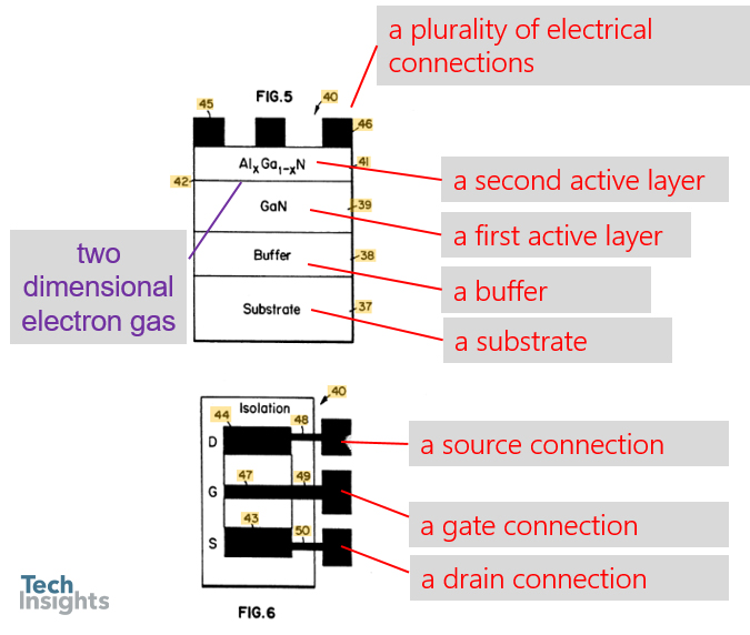
Figure 1 US5192987A Fig. 6
Through reverse engineering and patent analysis, we have been able to observe the key claim elements of the APA Optics patent ‘987 in multiple recent GaN power electronics products, including, for example, from International Rectifier, GaN Systems, Navitas, Infineon, Panasonic, Efficient Power Conversion, ONSemiconductor, Transphorm and Texas Instruments. We will review two selected examples here. Further examples are presented in our APEC 2020 presentation and TechInsights webinar.
International Rectifier was first to market with a GaN-on-Si power device, the IP2010PBF GaN-Based Power Stage, which was released in February 2010. International Rectifier was an American semiconductor company, founded in 1954. In 2015 it became part of Infineon. As shown in Figure 2, the IP2010PBF comprises a GaN-on-Si HEMT, co-packaged with an ASIC. The GaN-on-Si die features two separate power transistor blocks, that are wired in a high side/low side bridge configuration.
Figure 3 shows a cross-sectional TEM micrograph of the general structure of the IP2010PBF GaN-on-Si HEMT die. The key claim elements of the ‘987 patent have been mapped onto this image. Electrical measurements were also performed on this die, confirming that it operates as a transistor, as required by the ‘987 patent.
More detailed cross-sectional TEM micrographs of the contact and gate regions are presented in Figure 4. An ohmic metal 0 contact layer is used to make the source/drain electrical connection to the 2DEG that lies at the interface between the AlGaN second active layer and GaN first active layer. The device will feature normally-on operation, due to the presence of silicon nitride gate dielectric between the TiN gate material and the AlGaN. The presence of a gate dielectric is not explicitly described in the ‘987 patent, rather the patent describes the use of Schottky gate contacts. Schottky gates are not typically used for power electronics applications, but they are normally used for high frequency RF GaN HEMT devices.
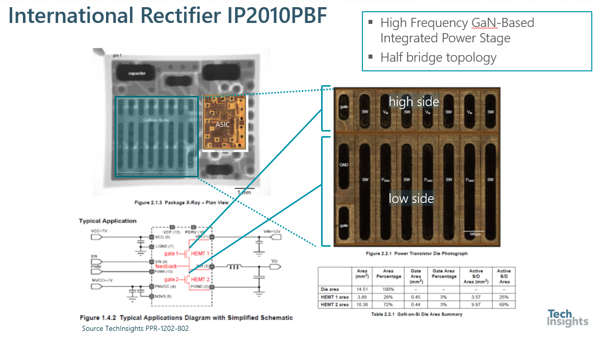
Figure 2 International Rectifier IP2010PBF GaN-Based Power Stage
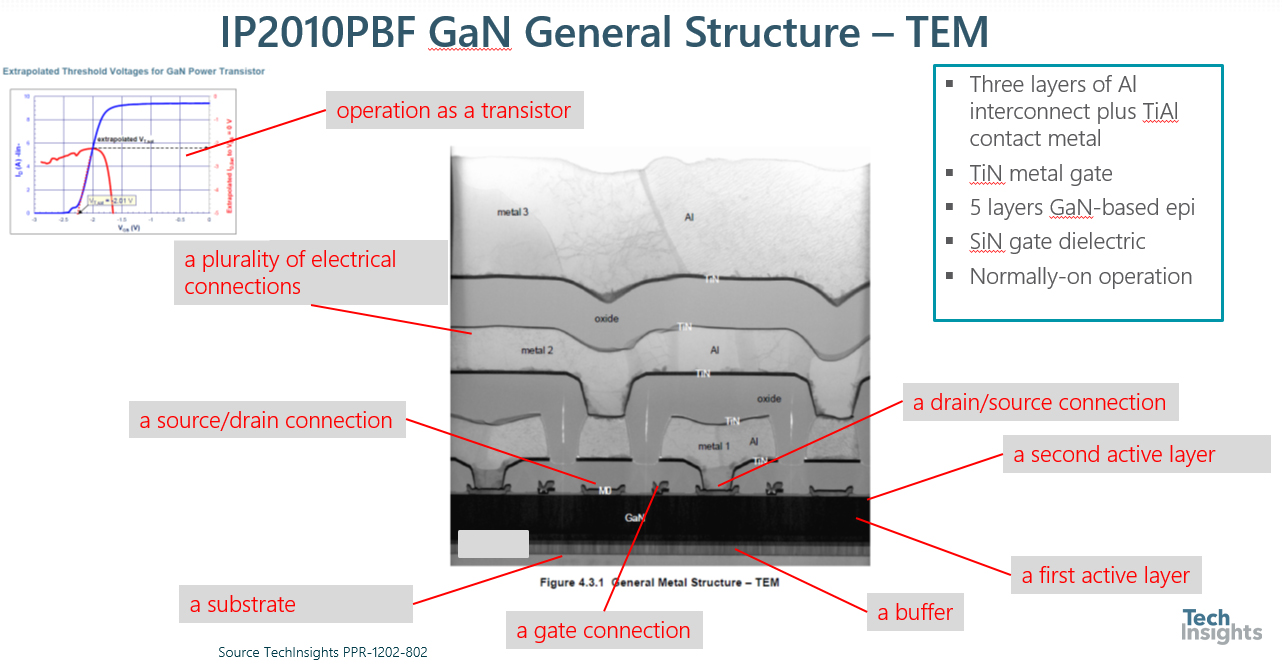
Figure 3 International Rectifier IP2010PBF General Device Structure – TEM
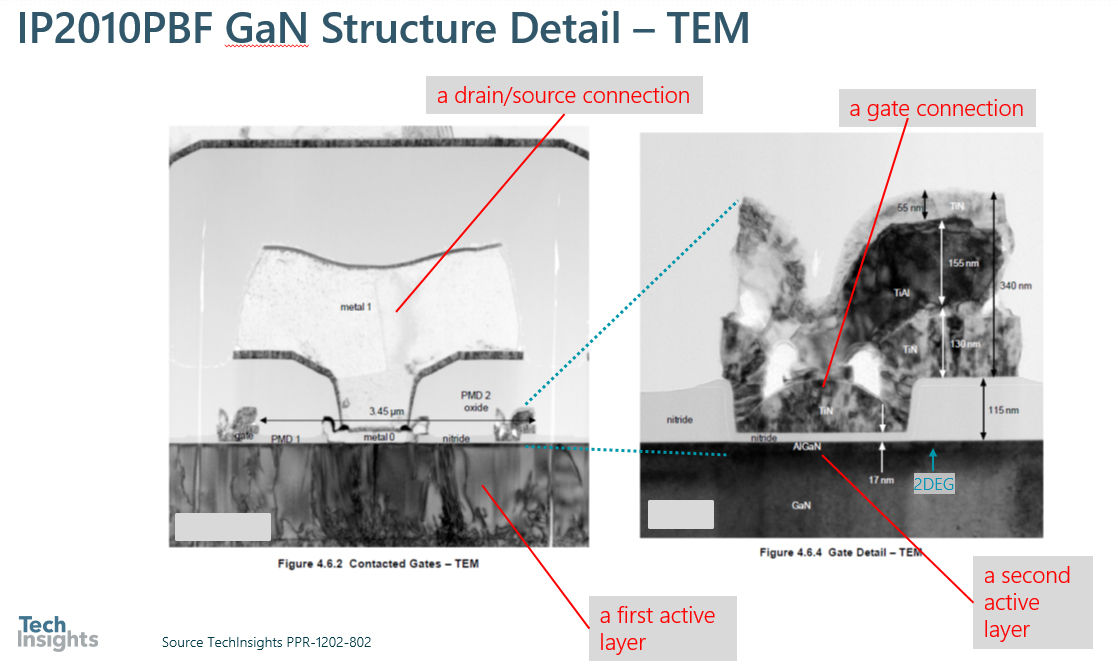
Figure 4 International Rectifier IP2010PBF General Device Structure – TEM Detail
Navitas Semiconductor is a US-based manufacturer of monolithically integrated (GaNFastTM) GaN-on-Si power ICs. They are based in El Segundo, California. At APEC in 2018, Navitas announced the NV6252 650 V integrated GaN half bridge, designed for active clamp flyback applications. TechInsights recently found the NV6252 device in the Aukey PA-U50 USB wall charger.
Figure 5 shows a photograph of the main PCB extracted from the Aukey PA-U50. Also shown in Figure 5 is a plan-view X-ray image of the NV6252 device. Two dies, with die markings NV6H002 and HV6L002, corresponding to the high side and low side transistors of the half bridge, respectively, are seen in the X-ray. A block diagram for the device, from the device datasheet, is shown below the X-ray image.
A photograph of the HV6H002 high side die, deprocessed to the transistor gate level, is presented in Figure 6. A power transistor block is observed in the bottom right corner of the die, while a block of analog circuitry wraps around the top and left side of the die. The presence of the large power transistor confirms that the device operates as transistor, as required by the ‘987 patent.
Figure 7 shows plan-view and cross-sectional SEM micrographs of transistors in the analog regions of the HV6L002 low side die found inside the NV6252. The key claim elements of the ‘987 patent have been mapped onto these images. Examination of the gate region of the transistors shows the presence of a mesa structure beneath the gate contact. This mesa is formed of P-type GaN and it forms the actual gate of the transistor. The presence of the P-type GaN in this mesa results in the depletion of the carriers in the 2DEG, thus giving rise to normally off (enhancement mode) operation. This concept was not anticipated in the original APA Optics patents, but is preferred in power electronics applications.
Finally, Figure 8 show cross-sectional SEM and TEM micrographs of the GaN-base epitaxy use to form both NV6252 dies. Ten layers of GaN-based epitaxy are used, including two super lattice structures. The key elements of the ‘987 patent continue to be supported, despite the additional complexity.
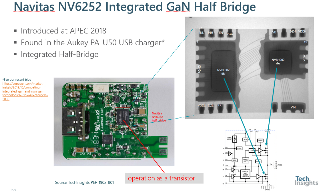
Figure 5 Navitas NV6252 Integrated GaN Half Bridge
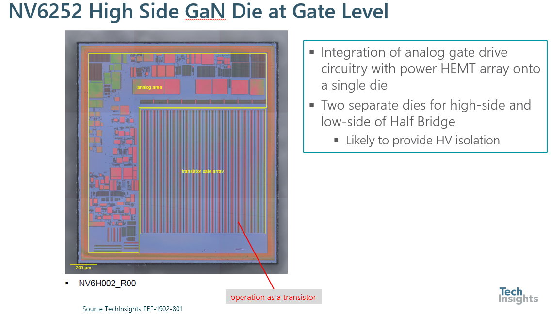
Figure 6 Navitas HV6H002 High-Side Die Layout
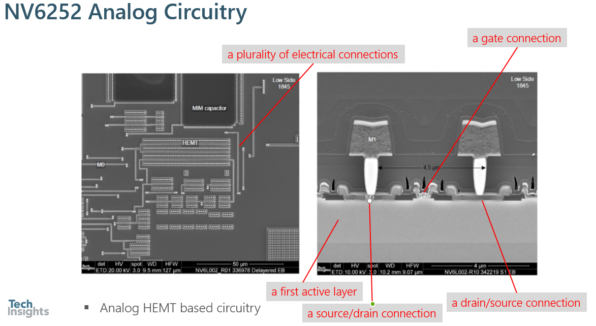
Figure 7 Navitas HV6L002 Low Side Die Analog Circuitry
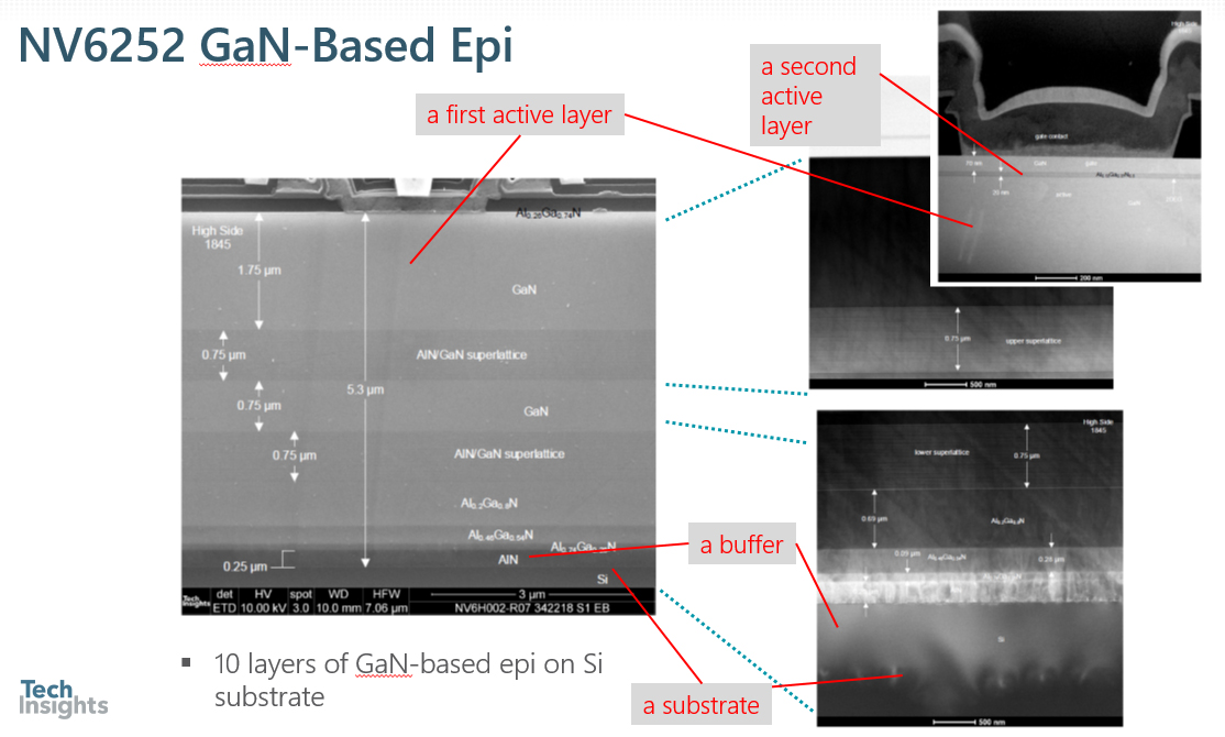
Figure 8 Navitas HV6H002 High Side Die GaN Epitaxial Structure
Gallium nitride-based power electronics is a rapidly emerging area of semiconductor technology. TechInsights is observing GaN-on-Si and also GaN-on-SiC power transistors in an increasing number of commercial products. Our results show that the seminal 1991 ‘987 GaN HEMT patent is now widely used. The concepts in the ‘978 patent, however, are now in the public domain. There has been considerable innovation since 1991, including the use of much more sophisticated GaN-based epitaxy, the use of Si and SiC substrates, instead of the sapphire (AlO) substrate described in the ‘987 patent abstract, the engineering of normally-off operation, and more recently the Panasonics hybrid gate injection (HD-GIT) technology. TechInsights continues to monitor this market and reports on key innovation as part of our Power Semiconductor Subscription program.


