Posted: April 24, 2017
Contributing Authors: Andy Wei
With the first set of Samsung Galaxy S8 teardowns, we have access now to the first SoCs produced on “10 nm” class technology. First to the 10 nm productization finish line is the Qualcomm Snapdragon 835, built on Samsung LSI Foundry’s 10 nm LPE technology. In parallel, Samsung’s own Exynos 8895 was released concurrently, and we expect to find these in our second set of Samsung Galaxy S8 teardowns.
The Qualcomm Snapdragon 835 has a die size of 72.3 mm2. Compared to the die size of the Snapdragon 820 at 113.7 mm2, this represents a 36% die size shrink. The Qualcomm Snapdragon 835 appears to be mainly a shrink of the Snapdragon 820/821 family, with upgrades in similar IP blocks, but no new major IP blocks have been added. There is, however, a major change in the CPUs. The Snapdragon 820 family used a very large area 2+2 big-little implementation which seemed out of place in a mobile applications processor. We suspect the Kyro was a re-use of cores designed for Qualcomm’s ARM server ambitions. The Snapdragon 835 uses a more ARM-like 4+4 big-little implementation in the Kyro 280, which are a derivative of the ARM Coretex-A73/A53 implementation we have already seen in the HiSilicon Kirin 960.
Complimentary Floor Plan (Annotated Die Images) & Product Brief - Samsung 10 nm Process
Qualcomm Snapdragon 820/821 on Samsung 14 LPP vs Snapdragon 835 on Samsung 10 LPE
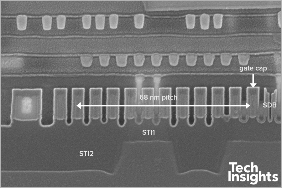
SEM cross section of the 10 nm
This major change in CPU skews the overall die size reduction, with the appearance of a more significant scale factor. However, looking at functional blocks with more minor changes, such as the Adreno 530 to Adreno 540 GPU MP unit, we see something closer to a 25% area scale. Whether this is indicative of the true scale factor, or this is the result of a concurrent increase in complexity to take advantage of the area scale, is not possible to determine without further analysis. To evaluate Qualcomm’s implementation of Samsung’s 10 nm LPE technology, we have to look very detailed at the functional block level and at the standard cell level, to gauge gate density gains and cost per gate scaling improvement. For an accurate assessment, we have launched extensive analyses at the functional block level, standard cell and utilization, process analysis, and transistor characterization. We can compare these to the analyses done on Samsung’s 14LPE and 14LPP for actual scale factor, cost scale, and performance differences. We will then compare it to our library of analyses on Intel, Apple, MediaTek, HiSilicon, etc.
This is an exciting time. In the midst of very high innovation to overcome physical scaling limits and maintain traditional cost and performance scaling, we are analyzing the first entry into the “10 nm” class technology. How does this fare compared to all the players at 14/16nm? And especially, how does this fit into Intel’s recent challenge to the industry to report actual transistor density as a technology metric? More detail to come as our analyses start to get down to the gate level.