
Prospects for Commercial High Voltage Silicon Carbide Devices - a Summary
SiC power devices have the potential to reach voltage ratings beyond 30 kV, yet today, SiC chip manufacturers are focussed on SiC MOSFETs and Schottky diodes from 600-1700 V. In this post, I shall explore the issues associated with high voltage (HV) SiC devices and try to answer the question as to why 10 kV devices still appear to be a little way from becoming a commercial reality.
Evidence of silicon carbide’s (SiC) potential as the next big thing in power electronics is before us today. A fast-growing number of companies have realised fast switching, low resistance Schottky diodes and MOSFETs from 600 V up to 1700 V. At this voltage range, these devices are optimal for the automotive and solar inverter applications (and much more besides), giving the power electronics designer a valuable tool in the development of small, light and efficient solutions.
However, the disruptive benefits of SiC do not begin and end in this very narrow voltage range, currently available. There are a host of applications, including traction, industrial machines, solid-state transformers, and several grid-level applications, that could benefit from a range of fully optimised SiC power devices with voltage ratings of up to 10 kV, or even higher. For example, in the implementation of HVDC conversion, SiC MOSFETs or IGBTs could replace Si IGBTs in VSC converters, making current solutions smaller and simpler by using fewer devices, or potentially extending the voltage range beyond what is currently achievable.
The materials properties of SiC allow it to withstand an electric field (voltage per unit length) 9x greater than silicon (Si) can. This ~9x ratio is a useful yardstick to predict the full potential of SiC technology using the existing Si market. For example, explore the devices available on the market and you will notice an equivalence in the on-resistance and current ratings of SiC MOSFETs rated 1200 V, with Si MOSFETs rated 150-200 V, as discussed in TechInsights recent annual power seminar. Therefore, with Si Superjunction MOSFET devices available up to 900 V, and Si IGBTs and thyristors available beyond 6 kV for IGBTs, one can foresee a much higher ceiling for SiC devices than the 1700 V of today’s MOSFETs. Voltages of up to 10 kV appear realisable for unipolar devices (MOSFETs and Schottkys), while bipolar devices (IGBTs and thyristors) could, at least in theory, surpass 30 kV. The SiC bipolar situation is an interesting topic of its own (maybe one for a future post!), but these do presently have some issues, namely the carrier lifetime of present SiC, and the absence of P+ substrates on the market.
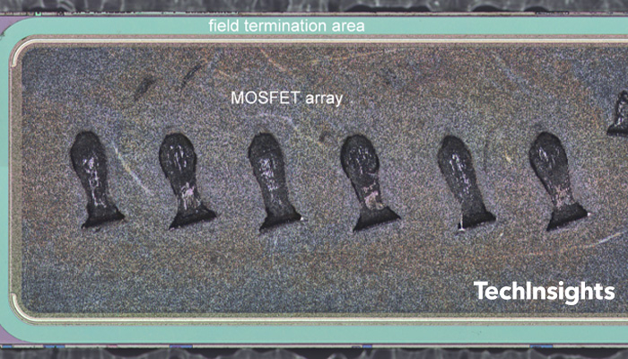
Figure 1 GeneSiC 3.3 kV MOSFET die
In reality, very few technological barriers prevent the upscaling of unipolar devices (Schottky diodes and MOSFETs) beyond 1700 V. Indeed, 3.3 kV devices are now available to buy, GeneSiC having already released 3.3 kV MOSFETs (up to 35 A as shown in Figure 1) and diodes (up to 5 A), while Mitsubishi Electric have integrated their own 3.3 kV products into their modules. While none of the major manufacturers have yet to release products >1700 V, every year at the international SiC conferences, Wolfspeed release data about their ‘medium voltage’ demonstrator devices, which include MOSFETs rated up to 15 kV and IGBTs and thyristors rated up to 30 kV.
One of the positive aspects to upscaling SiC MOSFETs, is the reduced dependence on trench gates to lower the on-resistance. This is because as the voltage rating of MOSFETs are increased, so too is the drift region resistance, which becomes an ever larger proportion of the total RDS,on. At 10 kV, this drift region resistance dwarfs the contributions from the substrate and the channel region, which means that the total RDS,on of even a planar device is very close to the unipolar limit of SiC, the lowest resistance achievable at a given voltage.
SiC materials costs scale up at with the voltage range, and these can be estimated, as follows. Based on the prices of thick epitaxy available to this author in 2020 (albeit on small order sizes), a SiC substrate with 100 µm of epitaxy, as required for 10 kV SiC MOSFET development, was over 4x the price of a 10 µm, 1200 V substrate. Factor in the chip size difference due to the larger termination, and the cost of a 10 kV, 50 A chip will be more than 6x more expensive than a 1200 V, 50 A chip. However, this is nothing new; chip costs have always scaled with voltage. As ever, economies of scale and competition would drive down these materials costs in a short time span, while higher prices will be more easily absorbed in these niche application spaces.
In the opinion of this author, the development of HV SiC device products is not being held back by technological barriers nor their costs. Some issues will need to be addressed to do with reliability at these voltages, but this is true of every new device class. Rather, in my opinion, the only obstacle to HV device development is the size and competition of the 600-1700 V market, with electric vehicles the driving force behind this. In contrast, the market size of HV applications, in traction or HVDC, is very small in comparison. Therefore, expansion into this area will require either the saturation of these larger markets, or for the more agile companies such as GeneSiC to continue to lead the way.
References
GeneSiC G2R120MT33J 3300 V 120 mΩ SiC MOSFET Power Floorplan Analysis (PFR-2102-801)
Infineon IMW65R107M1HxKSA1 650 V CoolSiC Power Essentials (PEF-2003-802)
Rohm SCT3022ALGC11 SiC MOSFET Power Essential (PEF-1905-802)
Dr Peter Gammon, Associate Professor (Reader) at the University of Warwick and the founder of PGC SiC Consultancy
Dr Peter Gammon has 15 years of experience in the design, fabrication and testing of SiC power devices, having published over 80 journal and conference papers on the subject. He is the Principle Investigator on major projects into the development of 10 kV SiC IGBTs, 3.3 kV SiC diodes and radiation hard SiC devices for satellite applications. The Power Electronics Applications and Technology in Energy Research group at the University of Warwick hosts state-of-the-art SiC facilities, including a SiC fabrication cleanroom, a SiC CVD reactor, a packaging lab, and a suite of facilities for the electrical characterisation and reliability testing of SiC power electronic devices.
Find content like this and more in the TechInsights Platform. Sign-up for free today.


