Latest SJ-MOSFET Technology, Can It Still Compete with Wide Bandgap?
Now both silicon carbide (SiC) and gallium nitride (GaN) products are having an impact in the marketplace, it is easy to think that there is no longer a place for silicon (Si) in power electronics. That the advantages offered by these wide bandgap (WBG) materials makes Si based devices obsolete. While it is almost a certainty that the market share for Si will decrease over the next decade relative to WBG, it seems unlikely to disappear anytime soon.
TechInsights' Power experts agree that (SiC) and gallium nitride (GaN) products show expansive system design applications such as:
- Date centers (Server power supplies, etc.)
- Power conditioners for photovoltaic generators
- Uninterruptible power Supply
- Automotive
- On Board Charge
- Inverter
- Industrial Motor Drive
- Renewable Energy
- Solar Inverter
- Switch Mode Power Supply
TechInsights has analysis planned for this device and wide bandgap technology.
Click below to sign up to read early findings and upcoming reports
TechInsights’ Power subscription products provide insights into emerging power semiconductor products as they enter mass production in high-volume applications.
Sign up to receive our free product brochure on TechInsights' Power Subscription
Silicon Carbide (SiC) and Gallium Nitride (GaN) Products vs. Silicon (Si) Technology
We recently analysed Toshiba’s latest 'DTMOS VI' superjunction (SJ) MOSFET, namely the TK065U65Z in TOLL package with Kelvin source. The Power Essentials Summary is available in the TechInsights platform. This device is rated at 650 V with a current of 38 A at 25° C and an on-resistance (RDSON) of 51 mΩ as quoted by Toshiba. converting this to specific on-resistance (RDSON*A) from our die measurement this gives 16.81 mΩ.cm2.
Toshiba DTMOS VI’ Superjunction (SJ) MOSFET, TK065U65Z Imaging and Specifications
Figure 1 shows a cross-section of the device MOSFET array, this looks like a standard vertical MOSFET design. It is only when looking at Figure 2 which shows relative dopant concentration the SJ structure can be observed.
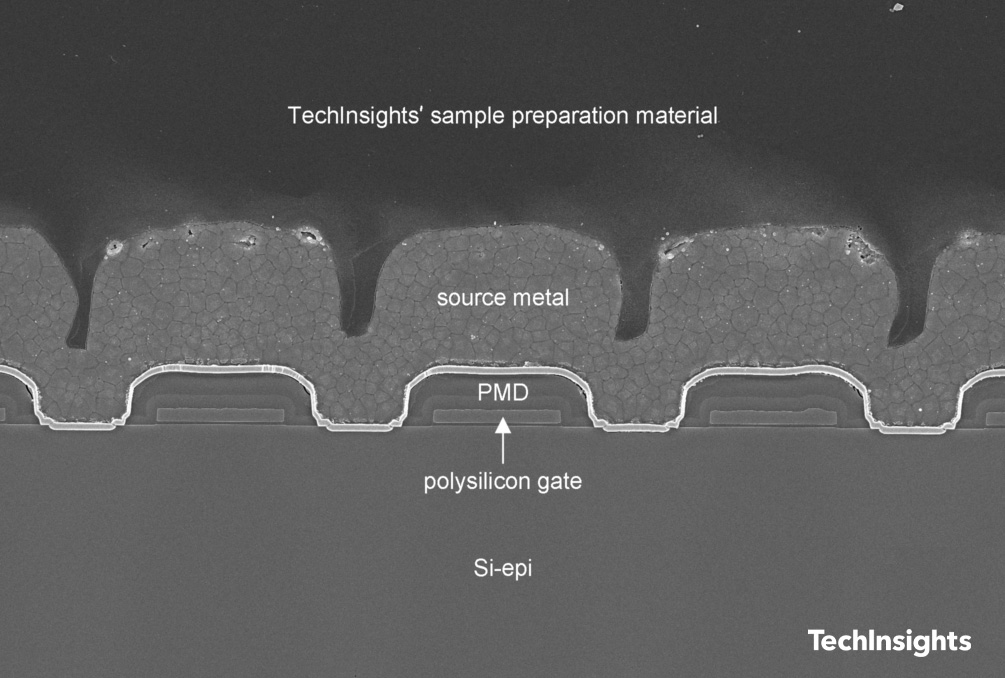
Figure 1. SEM cross-section image of Toshiba DTMOS VI SJ-MOSFET
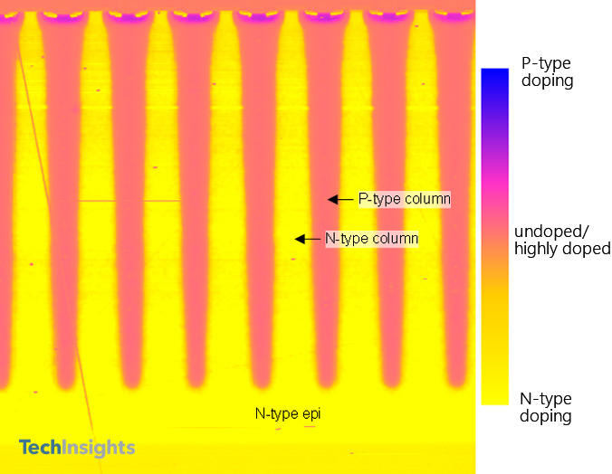
Figure 2. Scanning Capacitance Microscopy (SCM) image of Toshiba DTMOS VI SJ-MOSFET detailing relative dopant concentration
Comparison with DTMOS IV
In 2013 we analysed the Toshiba TK31J60W a 600 V, 31 A at 25° C SJ-MOSFET from the DTMOS IV generation, also in a Power Essentials report. The RDSON*A from our die measurement of this device gave 18.54 mΩ.cm2, approximately 10% higher than the newer device.
Although generally similar in structure the two most obvious differences between generations are:
- The older DTMOS IV device features a trench gate as opposed to planar.
- The cell layout is different with the DTMOS IV featuring one-dimensional stripes as opposed to the DTMOS VI with parallel disposed closed cells.
Figure 3 shows the gate of the DTMOS IV device protruding through the p-well into the N-type drift region, the channel being formed vertically along the p-well interface with trench. In the case of the DTMOS VI the gate sits on top of the Si die, overlapping the edge of the P-type columns to form a horizontal channel along the surface.
There are a couple of contrasting changes here:
- Implementation of a trench design tends to increase cell packing density. This might lead us to believe a higher current density and potentially a lower RDSON*A should be present in the earlier generation.
- Conversely the cell layout of the DTMOS VI device being of closed cell design gives more channel area across the die.
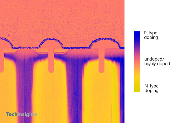
Figure 3. Scanning Capacitance Microscopy (SCM) image of Toshiba DTMOS IV SJ-MOSFET detailing relative dopant concentration
Clearly Toshiba has decided the planar layout is more suitable. The DTMOS VI does indeed have the lower RDSON*A, so in this case the cell layout must supersede the packing density enabled by a trench design. The exact reason they chose this is difficult to pinpoint but several factors may be in play:
- Trench designs tend to have a more complex fabrication process with a higher lithography mask count. Alignment to the charge balance columns is also crucial, but also applicable to a planar structure.
- The trade off with reliability and switching may be a factor, high electric fields at trench corners can pose a challenge, as for switching SJ-MOSFETs naturally have a large capacitance so there needs to be a careful balance of all relevant device metrics to ensure efficient and reliable operation. Particularly as these latest devices in TOLL package claim over 50% reduction in both turn-on and turn-off switching losses.
Competitiveness with Wide Bandgap (WBG) Alternatives
The 650 V class of power semiconductor devices is extremely competitive and is set to become even more so. Opportunities in the automotive market mean every material and manufacturer is trying to gain an advantage with unique solutions. While SiC and GaN naturally sit in this voltage class it is the SJ concept that allows silicon to reach this level. The charge balance columns cancelling charge within the MOSFET drift region under reverse bias, allowing heavier drift region doping giving lower and competitive RDSON values.
So how does the RDSON*A of the Toshiba DTMOS VI stack up against WBG competitors? Figure 4 shows a plot of RDSON*A vs. Breakdown Voltage as seen in our latest Power Essentials Analyst Briefing, available in the TechInsights Platform. The yellow starred device is the DTMOS VI with the blue circles representing SiC MOSFETs of various voltage ratings.
Clearly on this metric it cannot compete, we have observed 600 V Si SJ-MOSFETs with as low as 14 mΩ.cm2, however as shown in our Power Technology Roadmap it is difficult to envisage any SJ-MOSFET dipping below 10 mΩ.cm2 with the limits of scaling these devices being approached.
Where Si can still truly remain competitive is in cost. These devices are generally fabricated on 8" or even 12" wafers. SiC still only has volume manufacture on 6" substrates with a more expensive starting material and device fabrication cost. So, while WBG is pulling ahead in the performance race it would take cost equivalence of device manufacture to truly put silicon’s future in doubt.
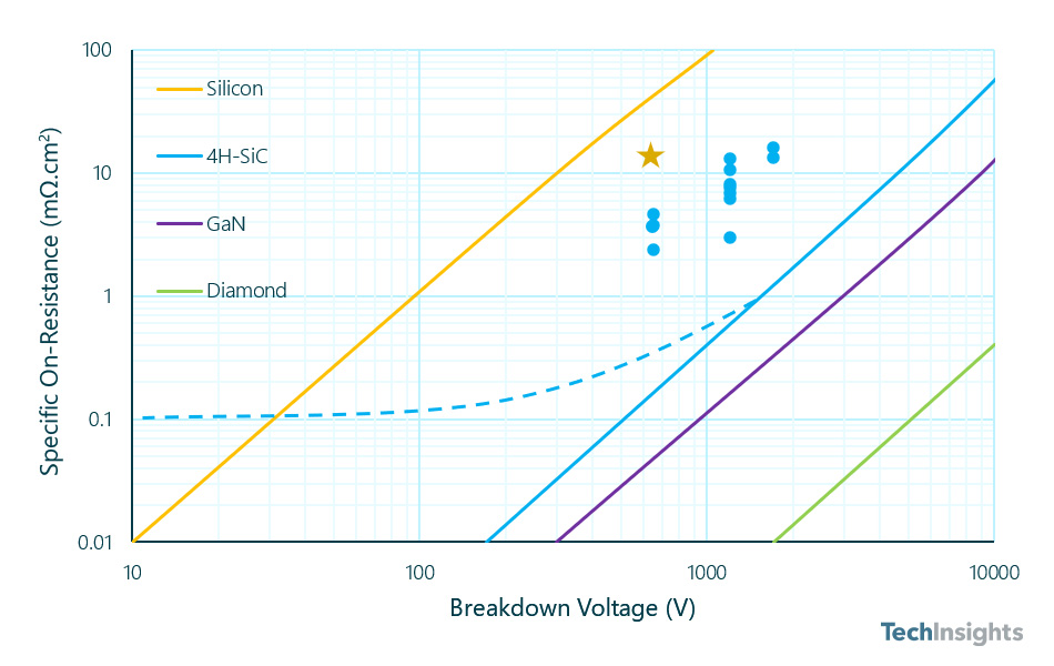
Figure 4. Comparison of RDSON*A for Toshiba SJ-MOSVET vs. SiC MOSFET competitors
References
- Toshiba Releases 650V Super Junction Power MOSFETs in TOLL Package (Toshiba Website) 2021.
- Toshiba DTMOS VI TK065U65Z 650 V Super Junction Power FET Power Essentials Summary (PEF-2103-801) TechInsights, 2021.
- Toshiba Announces Next-Generation Super Junction Technology for Power MOSFETs (Toshiba Website) 2012.
- ToshibaTK31J60W 600 V Super Junction MOSFET – Process Review Report (PPR-1212-901) TechInsights, 2013.
- Power Semiconductor Tri-Annual Briefing – Vol. 3 No. 1 (BRF-2101-802) TechInsights, 2021.
- Power Technology Roadmap (TechInsights) 2021.
Tags: Toshiba MOSFET Power Semiconductor
Interested in an Power Subscription?
TechInsights offers subscriptions to the broadest range of analysis and expert commentary. Contact us to learn about our many subscription offerings.


