Pat Gelsinger Takes us on a Trip Down Memory Lane – and a Look Ahead
Last November Intel held their Innovation Days, with opening keynote by CEO Pat Gelsinger. Taking the fiftieth anniversary this month of the Intel 4004 microprocessor as a starting point, he went through the evolution of transistor technology from 1971 until now, and briefly looked ahead at the upcoming nodes in the Intel roadmap. He subsequently posted this specific segment on LinkedIn, which saves us scrolling through the first half-hour of the keynote. A more detailed version has just been posted on the Intel YouTube channel.

Dick James

Intel CEO Pat Gelsinger - ‘Intel Innovation’ Keynote
Since I joined the business in 1970, working for Philips Semiconductor, this was very much a technology review of my career, and I couldn’t resist going through the sequence to show how remarkable the advances have been in the last fifty years.
It seems hard to believe, but back in 1971 we were using PMOS only, and 10-micron design rules! Polysilicon gate technology with self-aligned source/drains was a relatively recent introduction, replacing aluminum gates, and LOCOS (local oxidation of silicon) isolation was also coming into use. That’s what gives the taper to the oxide edge that we see below.
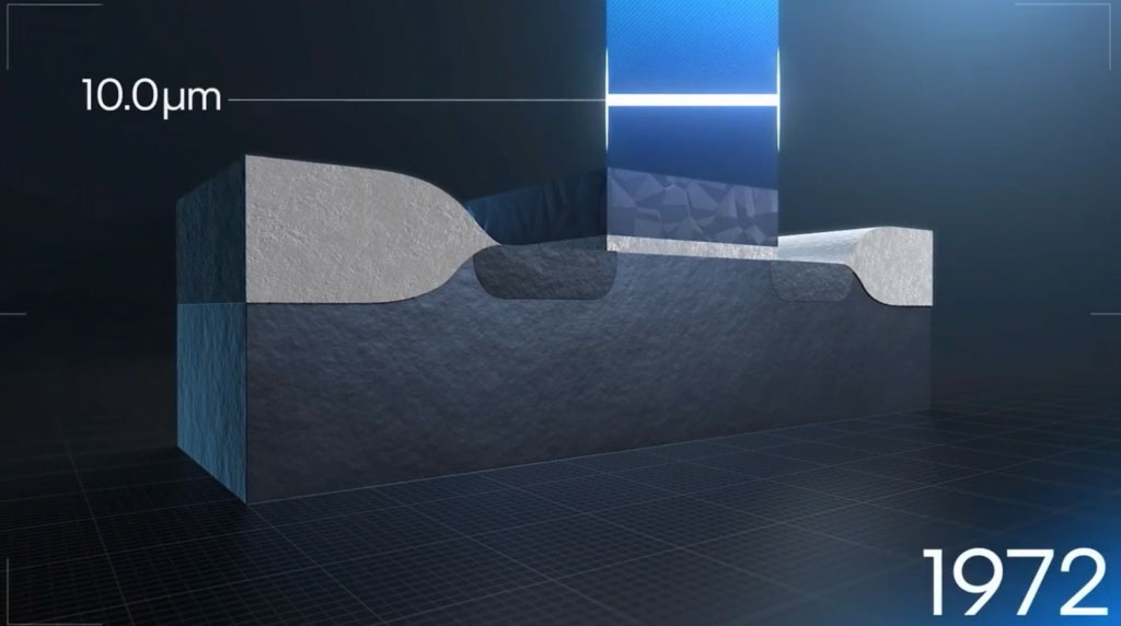
Lithography was done on the 2” wafers of the time by contact printing with manual alignment, and the rules of thumb were no more than five wafers per mask, and die size of no more than 5 mm per side.
On a personal note, I had my first tangle with patent enforcement back then, when I was asked by Philips legal to look at an Intel chip – they wanted to know if Intel was using LOCOS. We cross-sectioned the part, put it in our first, brand new SEM, and there it was! Philips at the time was more interested in technology exchange than licensing fees; as I remember it, the trade was the full process sequence and mask set for a 4K-DRAM. And no electronic imaging in those days, we did it all with Polaroid film.
Dennard scaling worked well through the rest of the decade, down to about 2 µm, when we started to see short-channel effects, and sidewall spacers and source/drain extensions were needed.
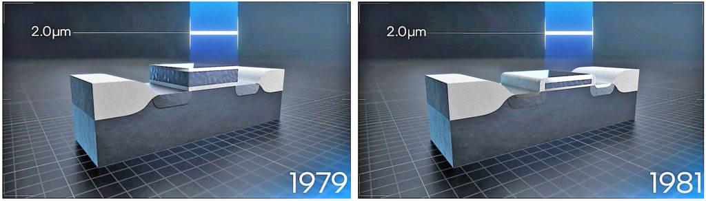
In the meantime, projection alignment and ion implantation were introduced, adding automation, accuracy and controllability to the whole process sequence.
We stayed with LOCOS until about the 0.35 µm node, when STI (shallow trench isolation) became the standard form of isolation.
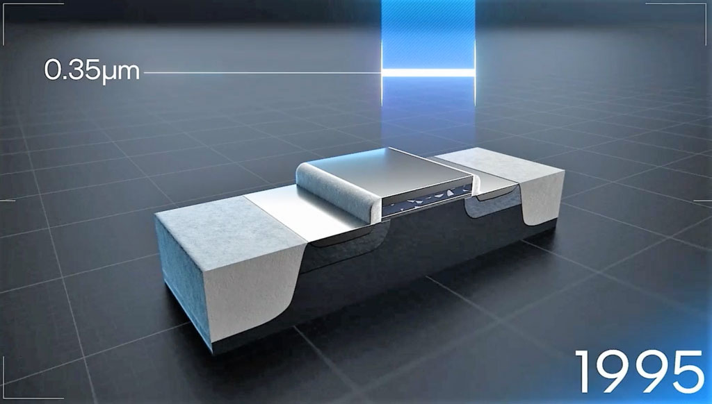
Of course, we also saw lots of changes in the back end, notably the introduction of CMP and tungsten contacts, enabling multi-level metals, and steppers took over lithography. Wafer size had evolved from the 2” of the early ‘70s, through 3”, 4”, and 6” to 8” (200 mm), with a few fabs running 5” in the interim.
As a general rule, for logic parts the gate length was used as the node or generation number down to ~0.35 – not universally accurate, but generally accepted. But at a quarter micron, things started to diverge, and gates shrank faster than the node number.
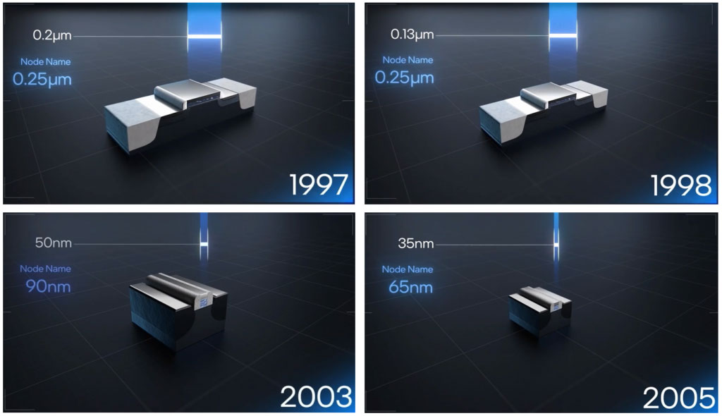
In 1998 IBM introduced copper metallization at the 180-nm node (gate length ~90 nm), and at 130 nm low-k dielectrics and 300-mm wafers came into use. At 90 nm Dennard scaling really did fail; the gate oxide had thinned down to ~1 nm, at which point it leaked current like a sieve, with consequent rise in leakage power. So to keep increasing performance, Intel increased carrier mobility by adding stress to the channel. They used tensile nitride for NMOS, and SiGe embedded in the source/drain to give compressive stress for PMOS.
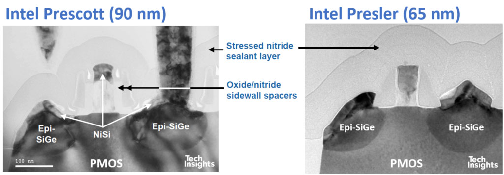
65 nm was essentially a shrink of 90 nm, optimizing stress to improve performance; the BIG change came at 45 nm, with high-k, metal gate (normally known now as HKMG).
It’s hard to see what’s going on here, so here are some TechInsights cross-sections of the 45-nm transistors [1]:
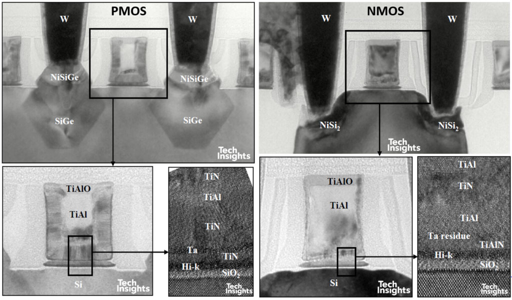
As you can see, a completely new philosophy of gate construction. A replacement metal gate (RMG) process is used, in which a dummy polysilicon gate is formed first on top of the high-k layer, then all the source/drain engineering is done (sidewall spacers through to contact etch-stop layer and dielectric fill); CMP back to expose the dummy gate, etch it out, and fill with the gate stacks.
There are extra subtleties in that the PMOS stack is built first over the whole wafer, then in the NMOS regions it is etched back to the tantalum layer, and the NMOS stack is deposited. We can also see that the embedded SiGe in the PMOS source/drains takes the (111) planes to improve stress transfer to the channel. Not visible in these images is a change from contacts through holes to contacts in trenches.
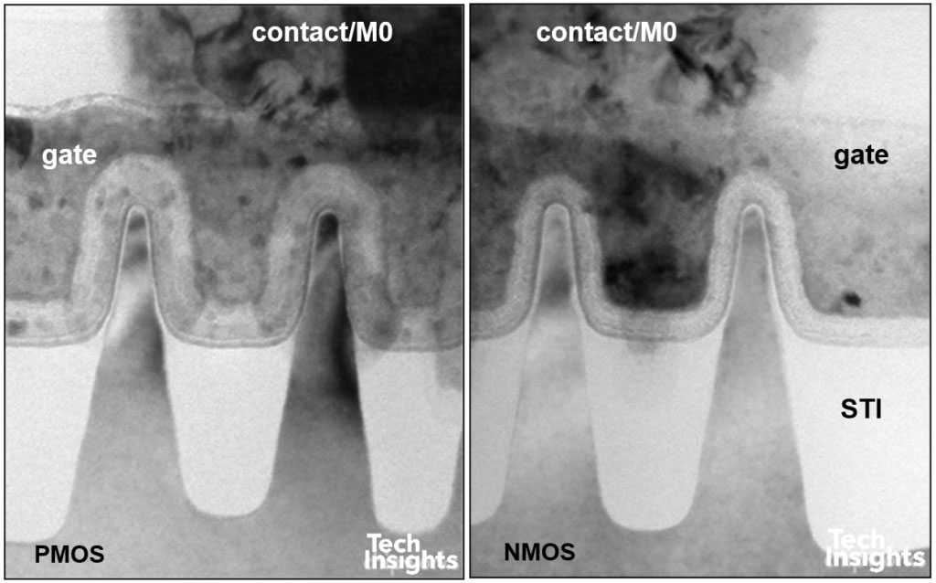
The 32-nm structure [2] is an evolution of the 45:
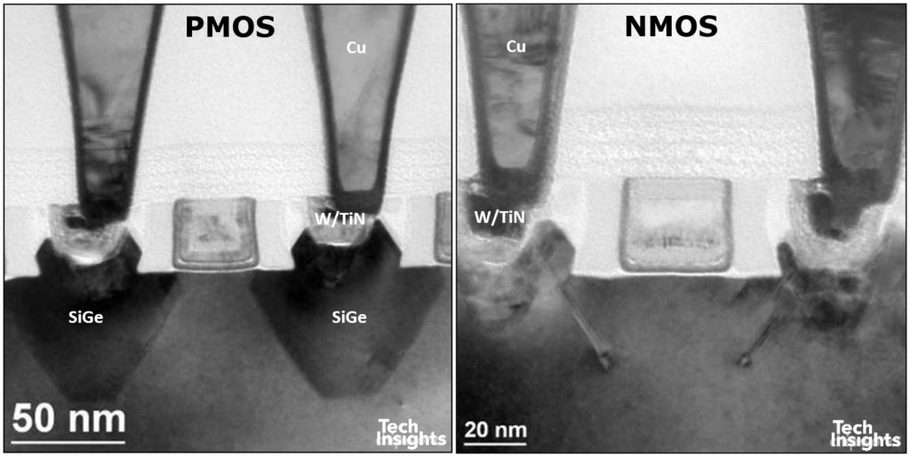
The sequence has changed slightly, since the high-k is laid down after the dummy gate is removed, but essentially the gate stacks are the same. The other notable feature is the polishing back of the tungsten contacts to stubs, with copper making the bulk of the contacts.
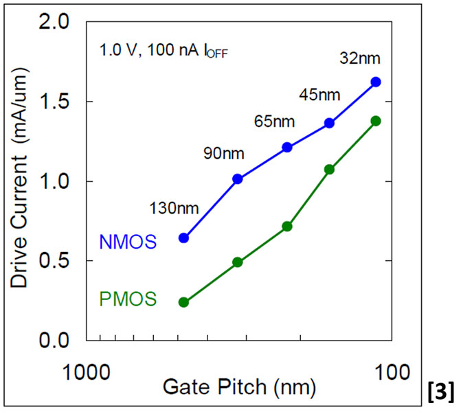
One of the benefits of the RMG process is that the removal of the dummy gate enhances the stress in the PMOS channel, improving the performance relative to NMOS. As shown in this plot from their IEDM 2009 [3] paper, the PMOS drive current increases noticeably from the 65-nm to the 45-nm node.
The next shrink was another huge architectural change, to a FinFET structure. Intel put the RMG gate stacks over a 3D fin-shaped substrate, giving gate control on three sides of the channel.
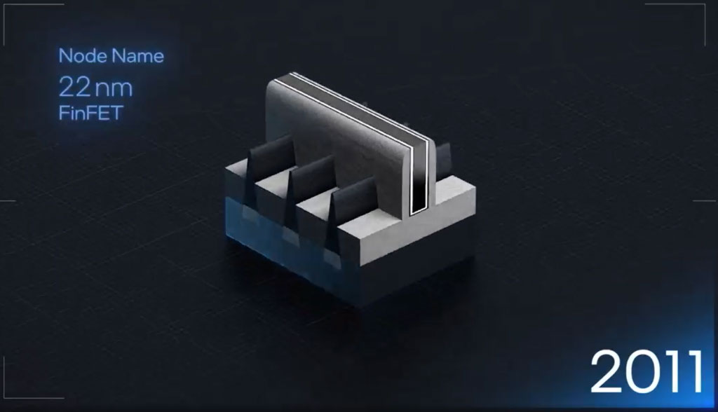
As seen in our TEM:
The tapered fins with rounded tops should be good for reliability, but the gate width is now defined by the wrap-around distance on the fin, forcing quantization of gate width, in this case to ~70 nm. The overall fin height is ~100 nm, and the fin width is 5 – 15 nm under the gate. The functional fin height is ~34 nm, giving us a gate width of ~70nm.
Having made the transition to FinFET, new generations followed, and we now have the Intel 7 Alder Lake part, released towards the end of last year.
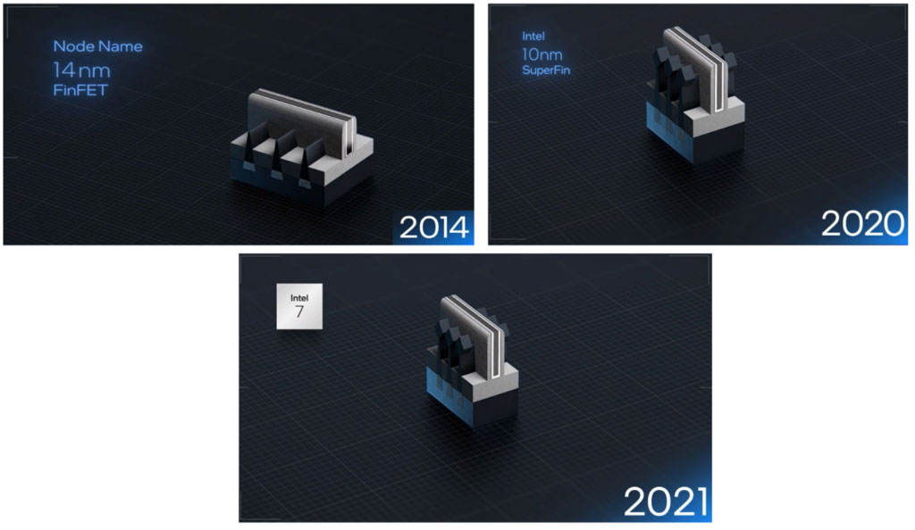
As you can see, there’s a six-year gap between the 14-nm and 10-nm nodes, and there were actually four iterations of 14-nm to get to 10-nm. In the meantime, fins became taller, more vertical, thinner, and closer together to give more drive current per unit area. We also had evolution of the gate stack to allow a greater range of threshold voltages. These are images of a 10-nm part:
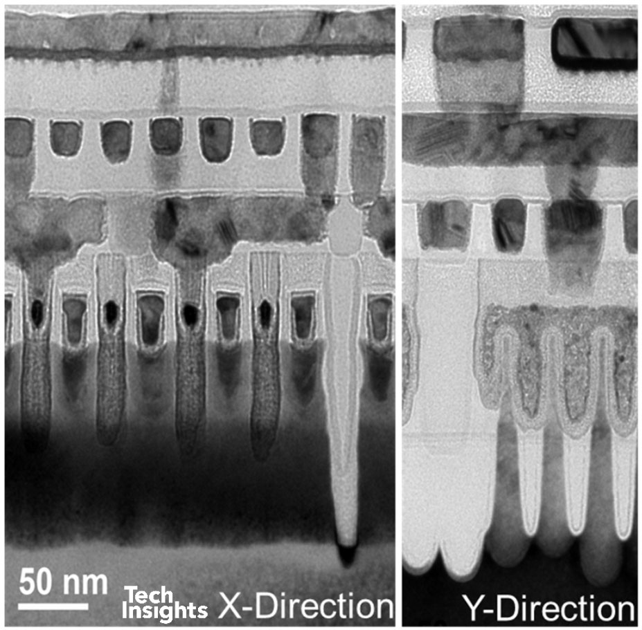
Alder Lake is currently under analysis...
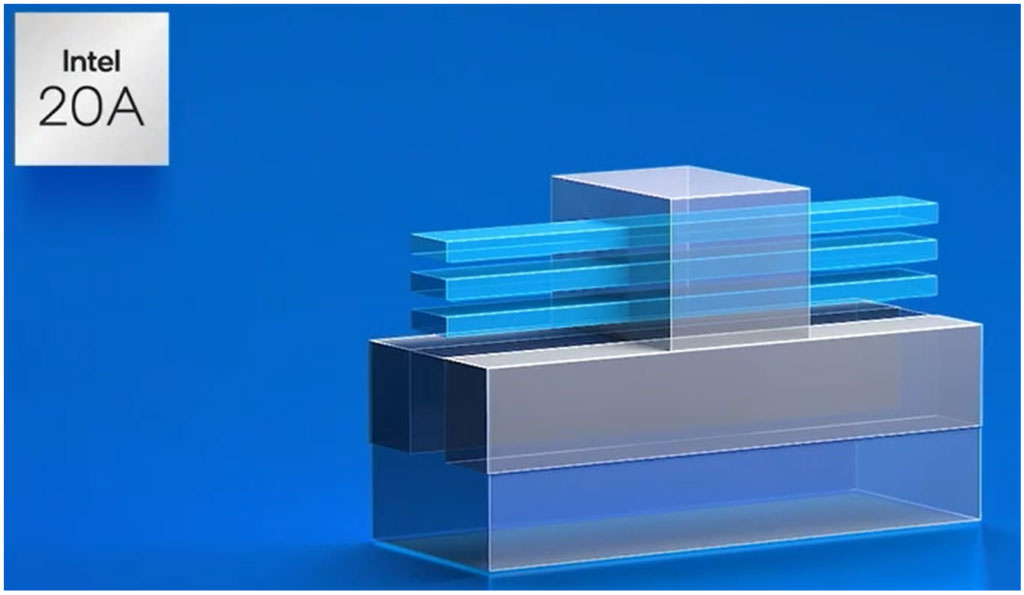
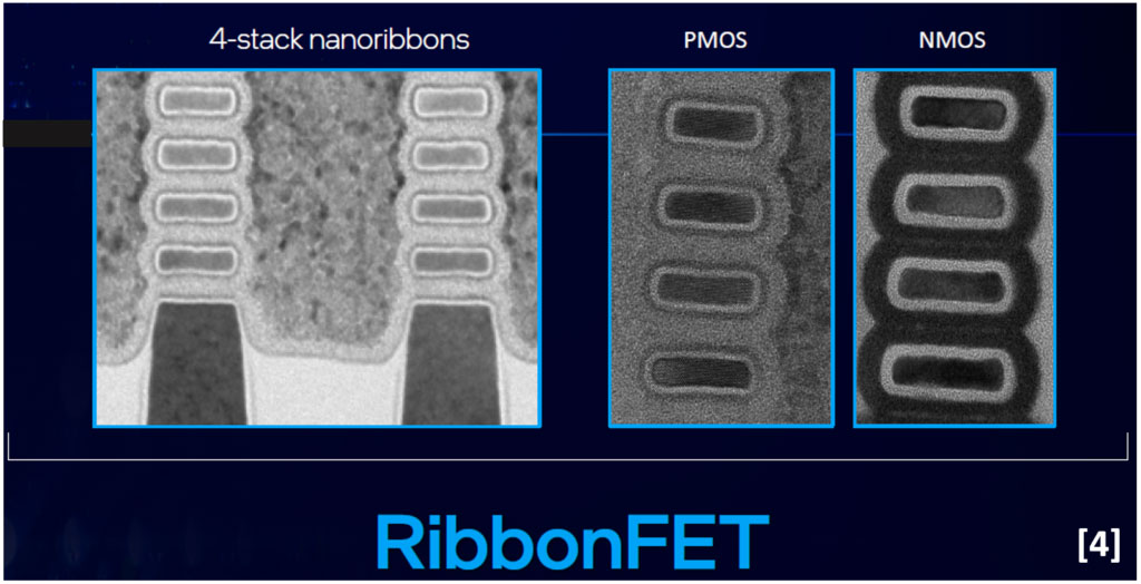
After running through the last 50 years of processing Pat Gelsinger looked ahead. Intel 4 and Intel 3 will continue to be finFETs. We will then see another architectural change at the 20A node (Intel’s nomenclature) to gate-all-around technology (GAA), in Intel’s parlance RibbonFETs, (nanosheets).
Apart from the extra channel control, the GAA structure adds flexibility since we can vary the width and number of the sheets, so gate width is no longer quantized as with finFETs.
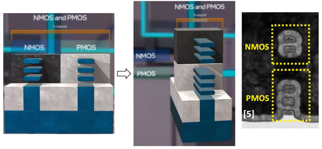
No mention was made of forksheet, imec’s introduction of a dielectric wall between NMOS and PMOS nanosheets; ultimately, to save area, we will get to stacked nanosheets, as described in Intel’s IEDM 2020 paper [5]:
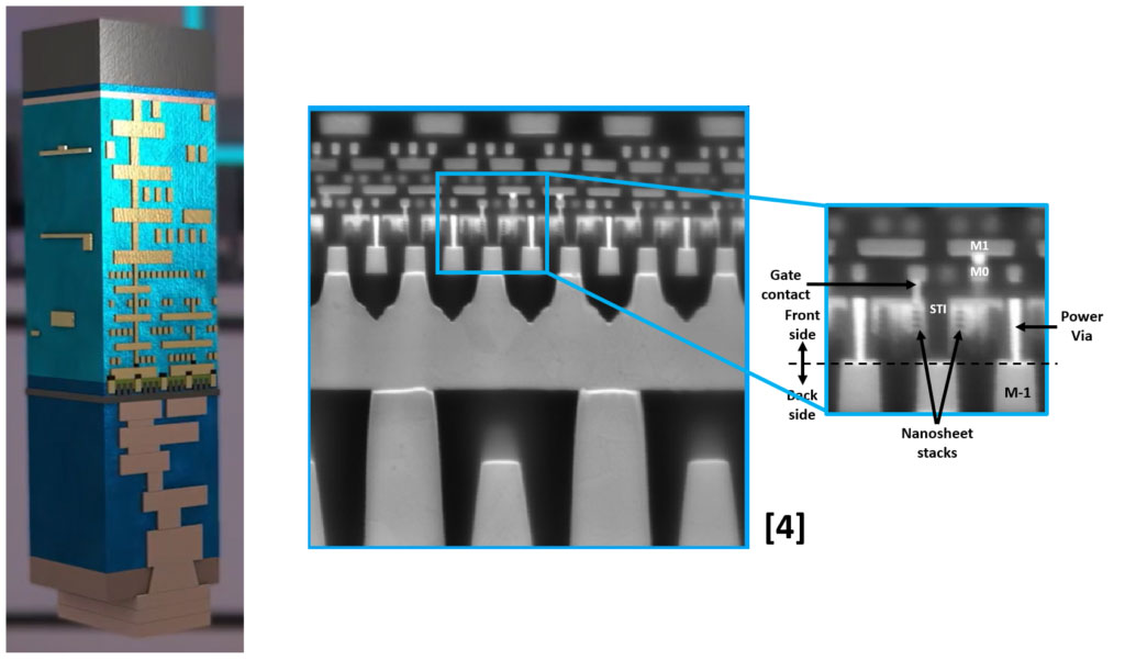
When the 20A GAA generation is launched, Intel is planning to use their PowerVia technology, putting the power delivery metallization on the backside of the die:
So in the last 50 years we have gone from the 10-micron generation to the 5-nanometer, shrinking 2000x, and to analyze them we have gone from optical microscopes to the latest aberration-corrected electron microscope.
And we still have plenty of generations to come!
Find content like this and more in the TechInsights Platform. Sign-up for free today.
References
- D. James, “From Strain to High-K/Metal Gate – the 65 – 45 nm Transition”, ASMC 2008
- D. James, “High-k/Metal Gates in Leading Edge Silicon Devices”, ASMC 2012
- P. Packan et al., “High Performance 32nm Logic Technology Featuring 2nd Generation High-k + Metal Gate Transistors”, IEDM 2009, pp. 659 – 662
- Intel Accelerated event, 26 July 2021
- C-Y Huang et al., “3-D Self-aligned Stacked NMOS-on-PMOS Nanoribbon Transistors for Continued Moore’s Law Scaling”, Proc IEDM 2020, paper 20.6, pp. 425-428


