4-Part Blog Series: The state of the art of smartphone imagers
Part 4: Non-Bayer CFA, Phase Detection Autofocus (PDAF)
Posted: July 30, 2019
Contributing Author: Ray Fontaine
Content adapted from TechInsights’ paper for the International Image Sensors Workshop (IISW) 2019
This blog series is structured in four parts:
(1) chip-stacking and chip-to-chip interconnect,
(2) pixel scaling and scaling enablers,
(3) active Si thickness and deep trench isolation (DTI) structures, and
(4) non-Bayer color filter arrays, and phase detection autofocus (PDAF).
The time allotted for the IISW talk did not permit discussion of optical stack trends, and it is not a topic that lends itself well to a text + figure discussion. That said, Figure 1 illustrates the optical stack thinning required for 0.8 µm generation pixels. To our knowledge, Samsung holds the world record thin optical stack at 1.17 µm, realized in its ISOCELL Plus technology platform.
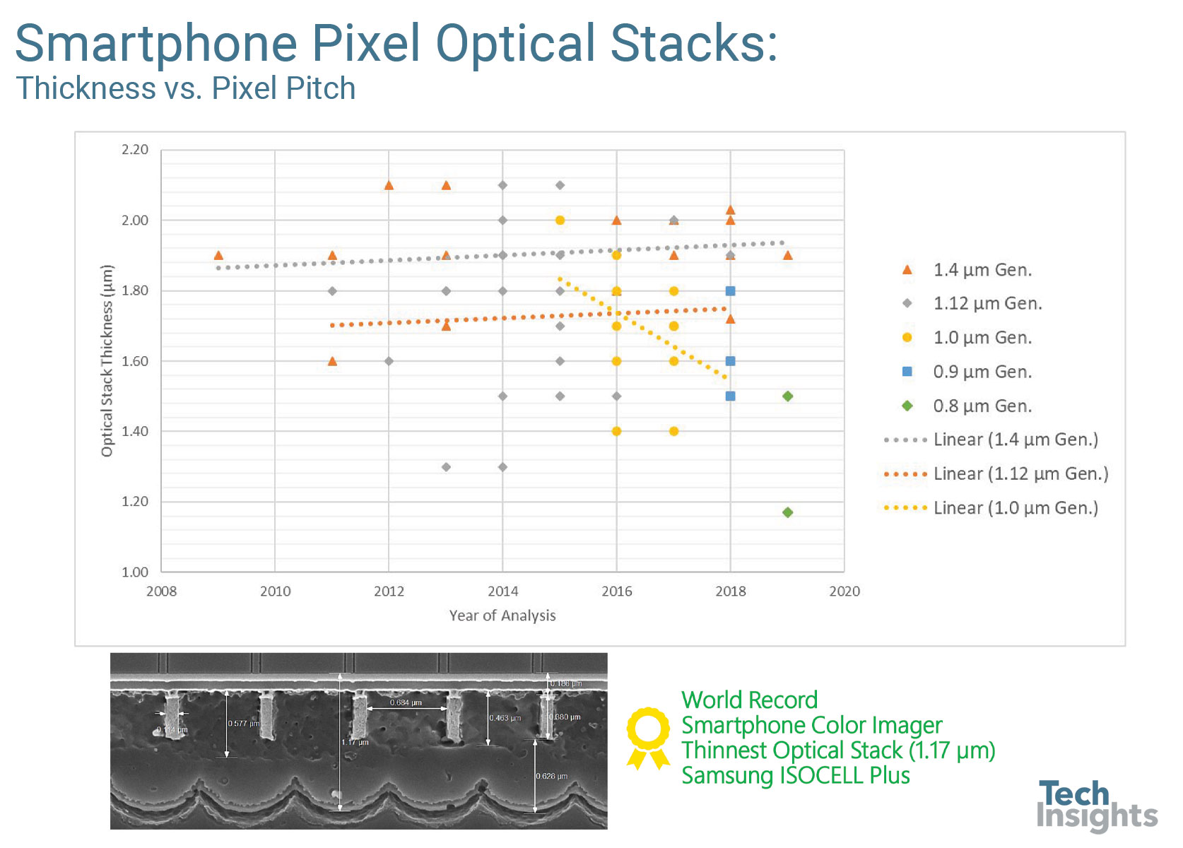
Figure 1: Optical Stack and Thickness Survey
The State-of-the-Art of Smartphone Imagers
Download our paper and slides from TechInsights' presentation at IISW 2019.
Bruce Bayer would be proud! His invention of the RGGB CFA remains the workhorse and best friend of the small pixel image sensor. We have documented several non-Bayer CFA schemes in use in larger pixels in different application spaces, but just a few in the small pixel space, as per Figure 2. OmniVision and Sony introduced RGBC/RGBW CFAs some time ago, and Samsung has used RWB. ON Semiconductor (Aptina) introduced a RYYB CFA in 2014 and we had not seen it elsewhere until recently, when Huawei featured it in its P30/P30 Pro sensor fabricated by Sony in 1.0 µm generation RYYB “Quad Bayer” pixels.
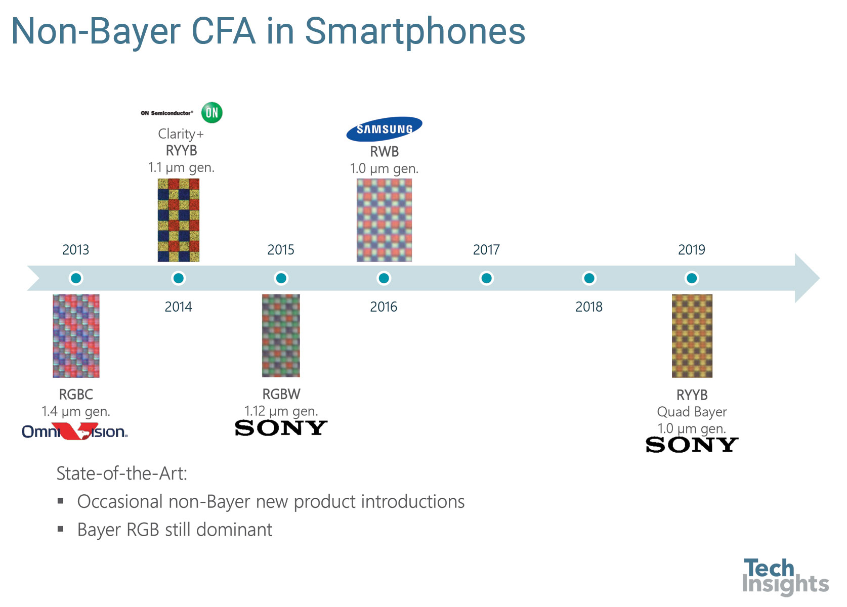
Figure 2: Non-Bayer CFA Survey
Beyond Bayer RGB, there has been a recent strategy in use to share a single color channel per 2x2 pixel grouping, as shown in Figure 3. Sony uses the term Quad Bayer to describe this scheme, while OmniVision calls its version 4-cell and Samsung adopted its Tetracell branding. Each scheme has been deployed across multiple pixel generations. Sony has 2x1 on-chip-lens (OCL) PDAF in use with Quad Bayer at the 0.8 µm generation, while Samsung uses clear replacement filters for its 0.8 µm generation masked PDAF pixels(!).
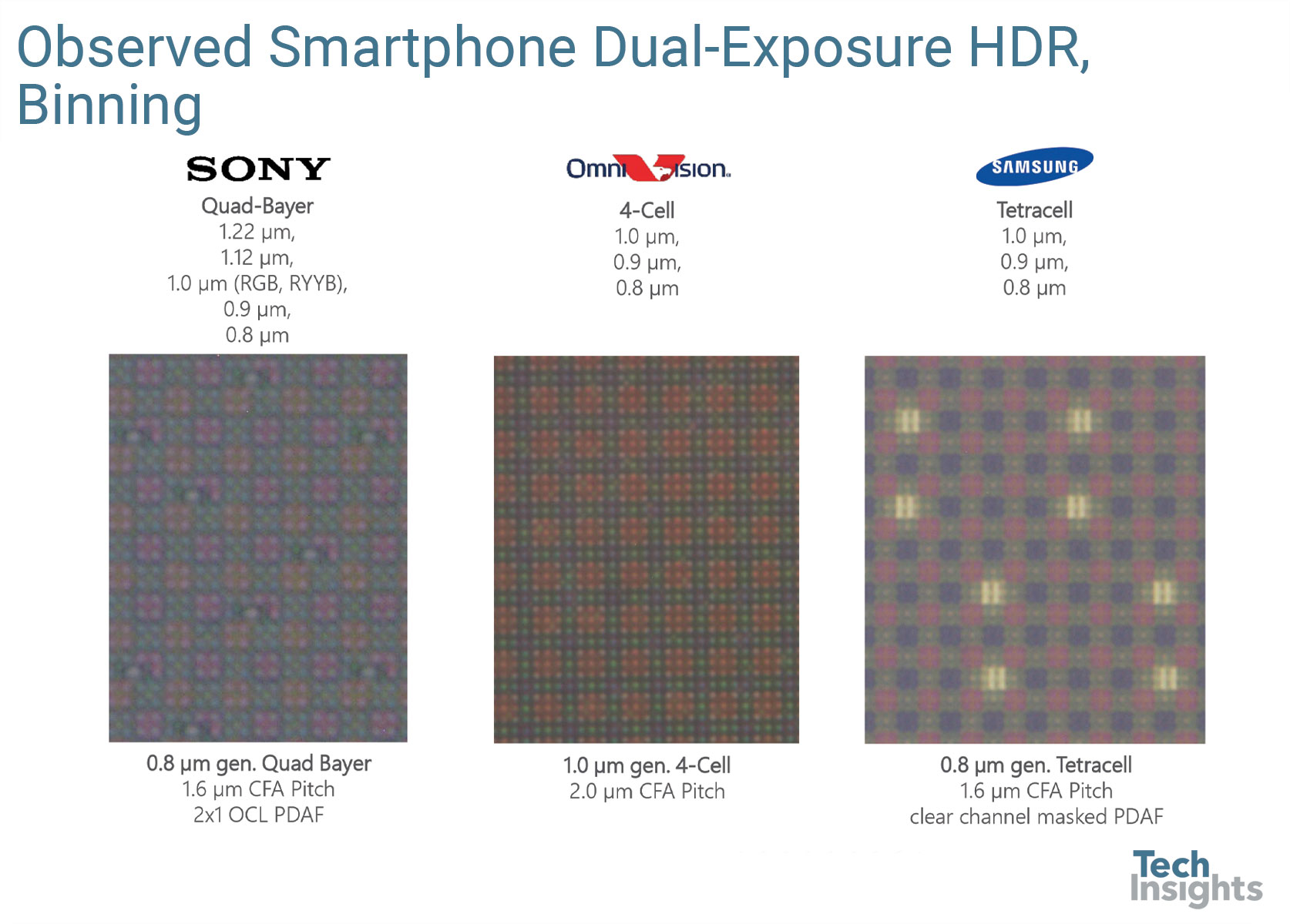
Figure 3: Quad Bayer with 2x1 OCL PDAF, 4-cell, Tetracell with Masked PDAF
The IISW talk concluded with a review of PDAF pixels in use in smartphones. The three solutions are summarized as masked, dual photodiode (dual PD) and 2x1 OCL. All were developed in larger pixel applications, primarily DSLR and mirrorless cameras. The first use of masked PDAF in smartphones was by Sony in 2014. The current record for smallest masked PDAF is Samsung’s 0.8 µm generation realized in ISOCELL Plus with Tetracell CFA.
Samsung’s Galaxy team dual sourced Sony and Samsung imagers in 2016 using 1.4 µm generation dual PD. TechInsights had documented Samsung’s 1.28 µm generation dual PD, as described in its VLSI 2017 paper, as being the smallest dual PD in use, but learned during the workshop this conclusion was incorrect. In fact, Samsung has 1.22 µm generation dual PD in production and we have just published our analysis to our report catalog.
Finally, 2x1 OCL is easily described as a double-wide microlens spanning two pixels within a row. This was originally developed by ON Semiconductor (Aptina), although we did not find parts for analysis until 2018. Sony emerged with this solution in iPhone in 2016 and we’ve since seen Samsung and OmniVision with its own solutions implemented in the 1.12 µm pixel generation. The smallest 2x1 OCL in use is used by Sony’s 0.8 µm generation.
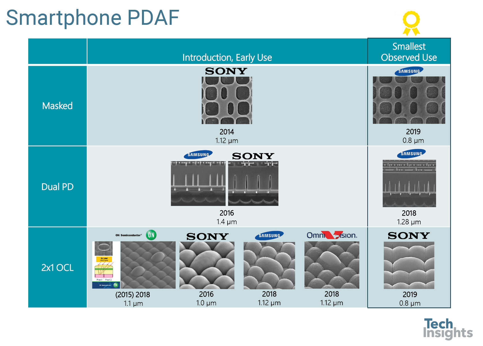
Figure 4: PDAF Classification, Introduction, Smallest in Use
We would like to thank the IISW co-chairs, Michelle (Yibing) Wang of Samsung and Daniel Van Blerkom of Forza-Ametek, the technical program chair, Vladimir Korobov of ON Semiconductor, the technical program committee members and board of directors for facilitating another world-class workshop. This was my 6th workshop, so 10th anniversary of the stop in Bergen, Norway. It is a remarkable format comparable to the Olympics where competitors declare a moment of peacetime to share the latest work in progress and field questions from attendees for the benefit of all.
TechInsights hosts the world’s most comprehensive catalog of image sensor competitive technical analysis reports and trends analyses, available through subscription 24x7 via cloud-based application. That said, we would be remiss if we did not comment on public domain resources of information, including the International Image Sensor Societies (IISS) site. The IISS site hosts a catalog of all previous workshop papers going back to 1973. Board members Eric Fossum, Albert Theuwissen and Vladimir Koifman each host invaluable content and blogs at http://ericfossum.com/, https://harvestimaging.com/blog/, and https://image-sensors-world.blogspot.com/ respectively.
Finally, this presentation content has been focused specifically on small-pixel smartphone imagers, which are maturing. We look forward to monitoring and reporting on the next generation smartphone imagers and optical sensors, and of course are covering the other imaging sub-sectors such as automotive, time-of-flight (ToF), machine vision, security/surveillance, etc. Despite being near the end of the small-pixel scaling roadmap, there are strong product road maps ahead and still a lot of work to be done by the imaging community! Figure 5 summarizes a few of the system and IC level technology domains we are monitoring as we document new technology elements reaching the mainstream.
What’s Next?
| System | Component/IC |
|---|---|
|
|
Figure 5: Technology Development Highlights
The Trusted Technical Intelligence Provider
TechInsights has been at the forefront of image sensor competitive technical intelligence since 2006, and have always been the first to report on key technology elements. All Top 10 image sensor design companies are our subscribers, and all Top 3 image sensor foundries are our subscribers.


