4-Part Blog Series: The State-of-the-Art of Smartphone Imagers
Part 1: Chip-stacking and chip-to-chip interconnect
Posted: July 09, 2019
Contributing Author: Ray Fontaine
Content adapted from TechInsights’ presentation for the International Image Sensors Workshop (IISW) 2019
TechInsights had the privilege of opening this year’s IISW workshop with a talk on the state-of-the-art of smartphone imagers. Smartphone imaging represents the highest-volume imaging application, and in most cases features the leading-edge in imaging technology elements. The outline of the talk was structured in four parts:
(1) chip-stacking and chip-to-chip interconnect,
(2) pixel scaling and scaling enablers,
(3) active Si thickness and deep trench isolation (DTI) structures, and
(4) non-Bayer color filter arrays, and phase detection autofocus (PDAF).
In this first blog of the series, posting chip-stacking and TSVs/Cu-Cu direct bonding interconnect will be presented, with the remaining topics released over the summer. Of course these are just the highlights pulled from the deeper analyses our subscribers have 24/7 access to under license to our image sensor subscription.
Stacked chip imagers are a requirement for flagship smartphone primary cameras. For comparison, Figure 1 shows the most recent iPhone primary camera two-die stacked imager (Sony, center), relative to the smallest and largest observed two-die stacks from OmniVision and Sony. There is no correlation between stacked chip area and method of vertical interconnect, but across this series we see butted Cu through silicon vias (TSV), Cu-Cu hybrid bonding, and dual TSVs in use.
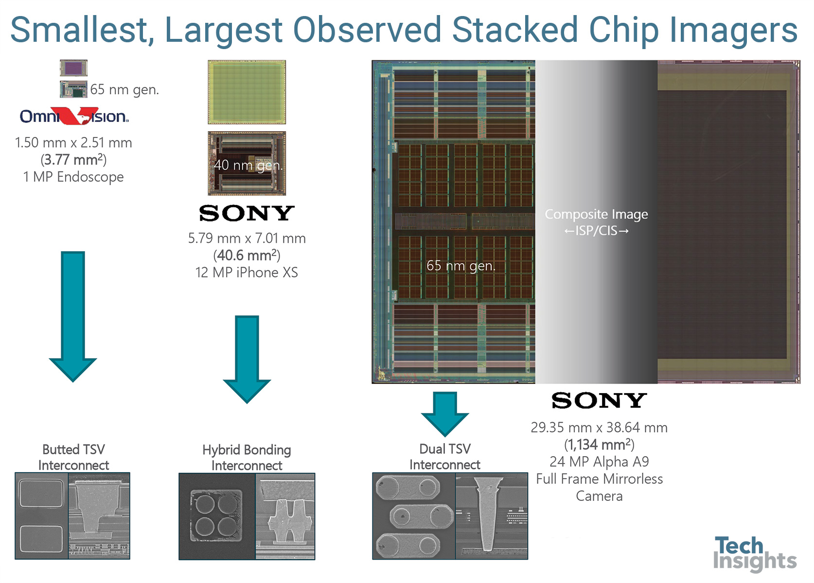
Figure 1: Smallest, Largest Observed Stacked Chip Imagers
The State-of-the-Art of Smartphone Imagers
Download our paper and slides from TechInsights' presentation at IISW 2019.
In Figure 2, the relative die sizes of stacked chip imagers from recent flagship Apple, Huawei and Samsung primary cameras is shown with the footprint of active chip-to-chip interconnect arrays annotated. Sony has big wins with its two-stacked imagers using 6.0 µm pitch Cu-Cu hybrid bonding. As demonstrated at IEDM 2018 and elsewhere, pixel level interconnect for small pixels is in development, but at this moment observed active Cu-Cu interconnect arrays serve only as TSV array replacements. Samsung’s solution integrates a DRAM die flip-chip mounted to the back of its two-die stack to form a triple stacked solution. Samsung prefers 6.0 µm TSVs for the imager to image signal processor (ISP) connections; further details are detailed in the next figure. The ISPs used in advanced Sony stacked imagers are fabricated in a 40 nm technology generation process, while the Samsung ISP is fabricated in a 28 nm technology generation process.
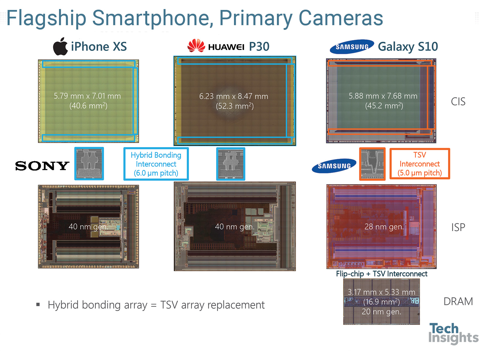
Figure 2: Flagship Smartphone, Primary Cameras
The next images are mostly recycled from previously published content but serve as a refresher for recent Sony and Samsung triple stacked imager structures from Samsung Galaxy smartphones. The Sony solution is a true three wafer stack interconnected with a full TSV flow which incorporates a redistribution (RDL) layer (not annotated) on the back of a thinned DRAM. The Samsung solution with flip-chip mounted DRAM incorporates two RDL layers and a high aspect ratio TSV through the ISP to achieve final connection from the DRAM to the frontside of the ISP.
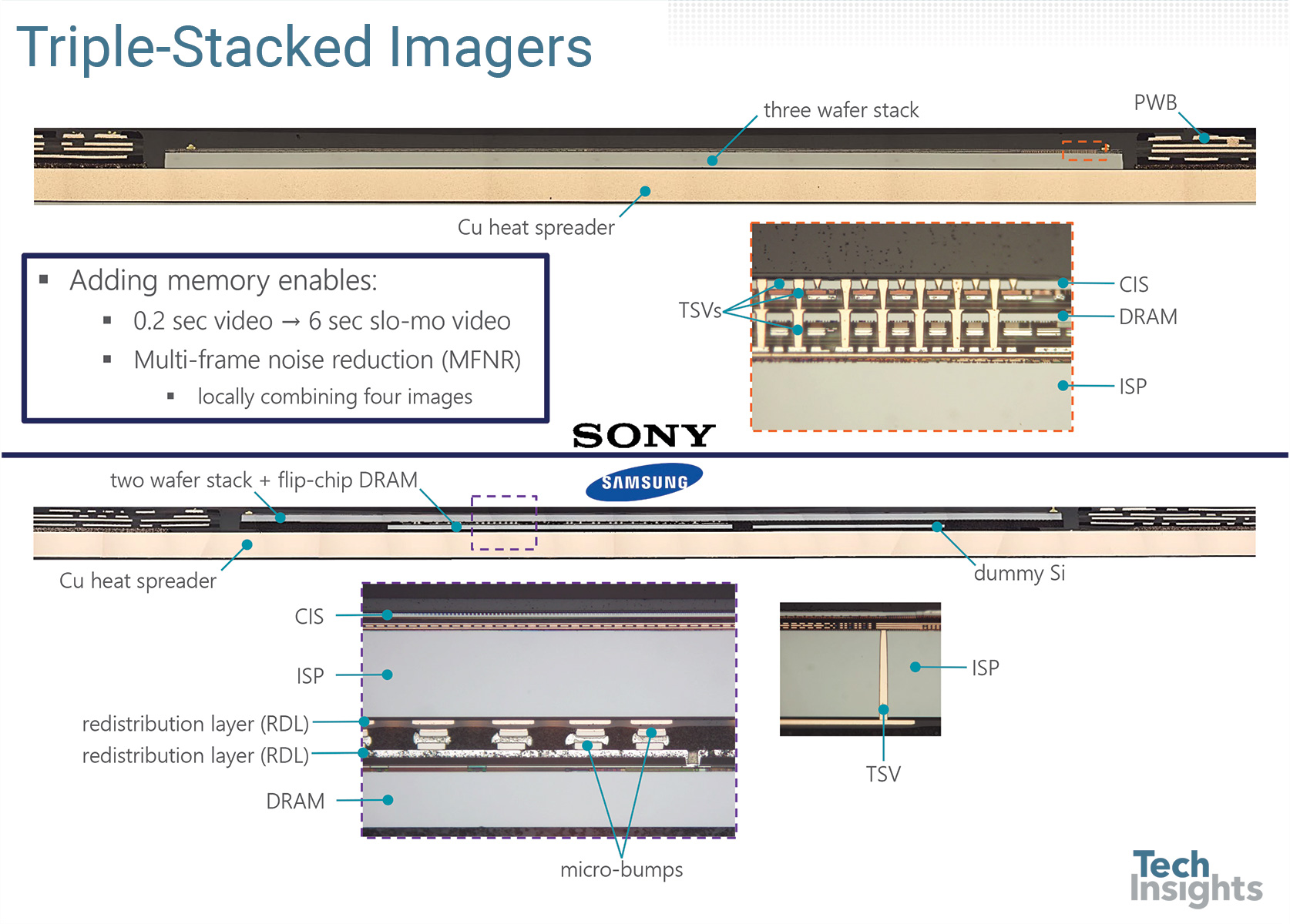
Figure 3: Triple-Stacked Imagers
If you attended the workshop, Figure 4 was skipped for brevity. It’s a high-level assessment of the distribution of front-illuminated (FI), back-illuminated (BI), stacked BI, and triple stacked BI configurations across selected applications. This analysis is mapped from our report catalog, but a full discussion is beyond the intent of this posting. Instead, it’s a good way to introduce Figure 5.
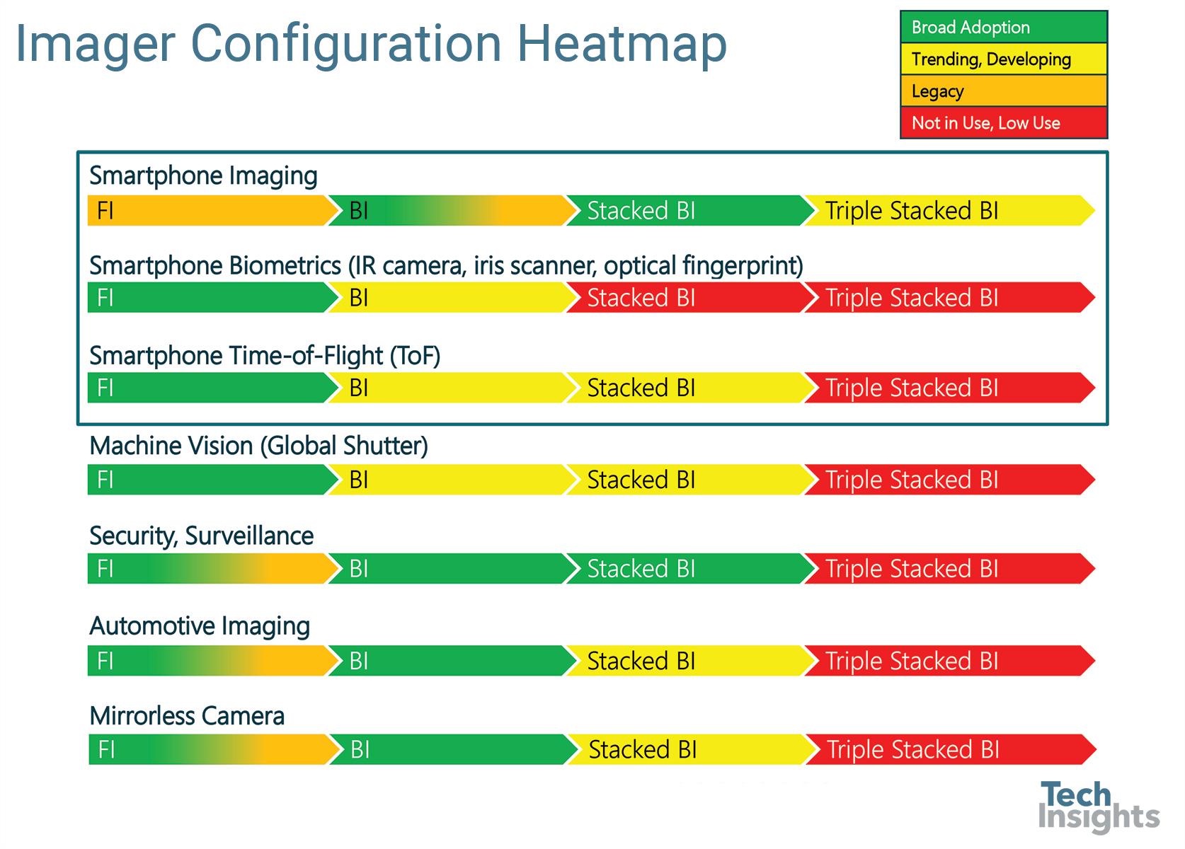
Figure 4: Imager Configuration Heatmap
A brief history of stacked smartphone imagers from three leaders is illustrated as follows. Sony launched its first stacked chips with dual TSVs and evolved to a single TSV structure. Its first generation 6 µm pitch Cu-Cu hybrid bonding is still in wide use however we’ve just documented in 2019 an evolution to 3.1 µm pitch Cu-Cu hybrid bonding in its 0.8 µm pixel generation sensor. To our knowledge this is the world record for imager Cu-Cu hybrid bonding pitch. OmniVision and foundry partners have produced butted TSV, single TSV and Cu-Cu direct hybrid bond interconnects. To our knowledge, TSMC holds the world record for imager single TSV pitch at 4.0 µm. W-filled TSVs are the preferred interconnect choice for Samsung stacked imagers and we’ve documented 5.0 µm TSVs in its stacked imagers.
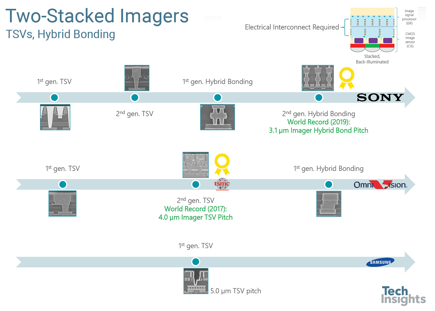
Figure 5: Two-Stacked Imagers
We’ll take a break here and resume posting the IISW 2019 presentation contents as a series of blog postings over the summer. The next topic discussed will be the trend of small pixel scaling and related technology enablers.
The Trusted Technical Intelligence Provider
TechInsights has been at the forefront of image sensor competitive technical intelligence since 2006, and have always been the first to report on key technology elements. All Top 10 image sensor design companies are our subscribers, and all Top 3 image sensor foundries are our subscribers.


