Packaging Approaches to Gallium Nitride (GaN) Products
In 2021 the power semiconductor subscription at TechInsights launched a new product – ‘Power Packaging Analysis’. It is true for any semiconductor that the package is important for electrical isolation, product robustness and thermal management. For power semiconductors it is crucial. With the shift to wide-bandgap (WBG) materials such as silicon carbide (SiC) and gallium nitride (GaN), the increased current density and switching speeds these materials enable come with more stringent requirements.

Stephen Russell
Packaging Approaches to Gallium Nitride (GaN) Products
When dealing with GaN there are two additional considerations compared to silicon (Si) to optimise the device performance.
- GaN’s potential for fast switching, enabled by the two-dimensional electron gas (2DEG) channel at the GaN/AlGaN heterojunction interface.
- GaN’s relatively poor thermal conductivity. (~1.3 W/cm.K at 300 K, compared to silicon’s 1.49 W/cm.K and silicon carbide’s 3.7 W/cm.K)
Granted the bulk thermal conductivity is not significantly lower than silicon, but remember the higher current density – which is confined to a small region around the heterojunction.
Find content like this and more in the TechInsights Platform. Sign-up for free today.
Incremental Improvements
Although not ideal, legacy Si packages can and have been used to package WBG devices such as GaN. The TO-247 package is commonly used for silicon (Si) power MOSFETs and IGBTs, wherein the bottom of the die (so drain or collector contact) is bonded directly to a copper lead frame. When used in an application it is standard practice to mount this directly to a heatsink using the through hole opening.
This idea transfers reasonably well to a SiC MOSFET, they share a similar structure to their Si counterparts. GaN devices today are of a lateral design however, with the structure confined to the top of the die. Meaning much of the cooling benefit is lost. Another challenge the lateral GaN structure gives is layout related. All three device terminals (gate, source and drain) require pads and associated bond wires to fit around the die somehow.
A major selling point of using GaN is the ability to shrink product size. So, for a Si power FET found in a discrete TO-247 package, the same voltage and current rating GaN counterpart could be packaged in a surface mount QFN style package.
Unfortunately, this makes matters more challenging from a thermal management point of view. Remember a higher current density will require more stringent packaging solutions – smaller chips in a QFN need more thermal management not less. Today some manufacturers have begun to adapt these packages to suit their application.
See the Navitas NV6128 for example, this is a monolithically integrated GaN IC which suits the multiple output ports of a QFN package. The package bottom with ports annotated can be seen in Figure 1 from a recent power packaging report. The GaN die sits to one side on top of the cooling pad ‘CP’. This is clearly sufficient for this device; although it is interesting to note that for Navitas’ recently announced 3rd generation GaN with ‘GaN Sense’ they have put a focus on control circuitry to sense and control operating temperature.
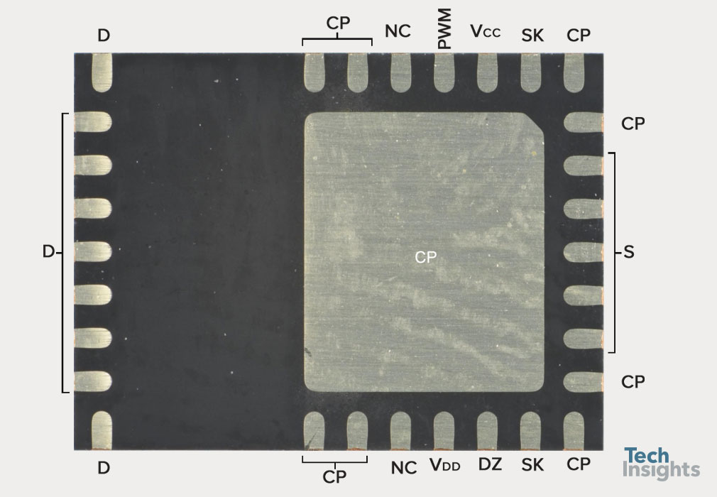
Figure 1. Bottom of Navitas NV6128 with cooling pad visible.
Bespoke Solutions
Other manufacturers have begun to focus on GaN specific packaging solutions. GaN Systems for example have several packages where the die is embedded within. See Figure 2 for a cross-sectional image of the GS61008P from another recent power packaging report. Copper pillars connect directly to the top and bottom of the die with package vias then connect these to a heatsink.
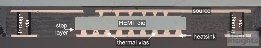
Figure 2. GaN Systems GS61008P package cross-section.
How about the other consideration for GaN – optimising switching performance? Minimising package parasitic components is key to this. Efficient Power Conversion (EPC) take the radical approach of essentially having no package or a ‘wafer scale’ package. This is essentially just a passivated die with solder bumps/bars for direct attachment to a PCB (see Figure 3 from a a recent GaN floorplan report). Parasitic inductance is minimised due to the lack of associated bondwires, sources of thermal resistance from interfaces are also minimised as the die can itself in theory be bonded directly to a heatsink. Care and potentially specialised conditions will need to be taken by the circuit designer in die attach, however. EPC recently broke from this tradition and announced a packaged device, the EPC2302. This case with exposed top appears to be a compromise somewhere between wafer scale and an embedded die.
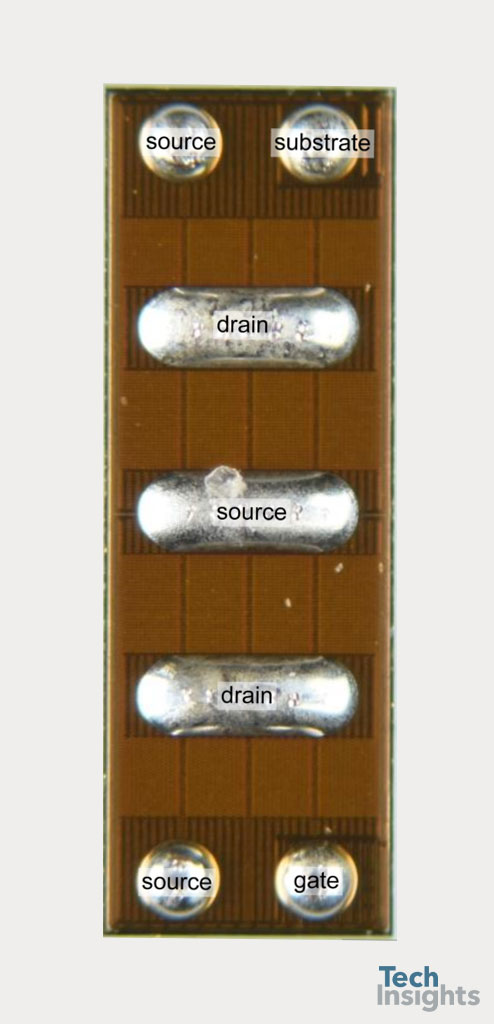
Figure 3. EPC2019 die bottom with solder bumps/bars visible.
Find content like this and more in the TechInsights Platform. Sign-up for free today.
Another approach to reducing inductance comes from Nexperia with their ‘copper clip’ design. Their idea to minimise parasitic inductance is again by removing bondwires. Figure 4 shows a cross-section of the PSMN3R9 Si MOSFET from a power packaging report (note this package has also been applied to GaN devices).
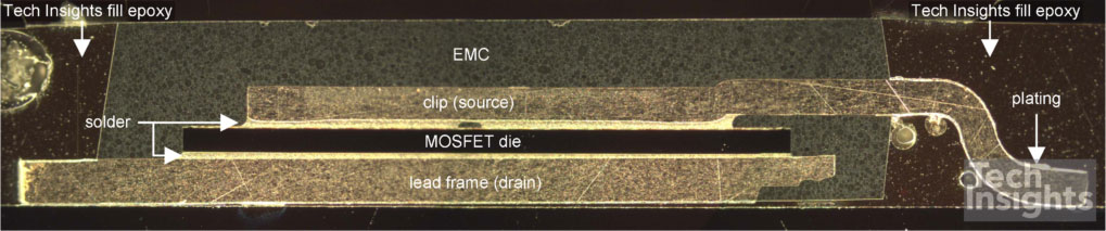
Figure 4. Nexperia PSMN3R9 package cross-section.
Figure 5 shows a plan view image of this device, it has been jet-etched to expose the copper clip. This is soldered directly to the source contact of the die.
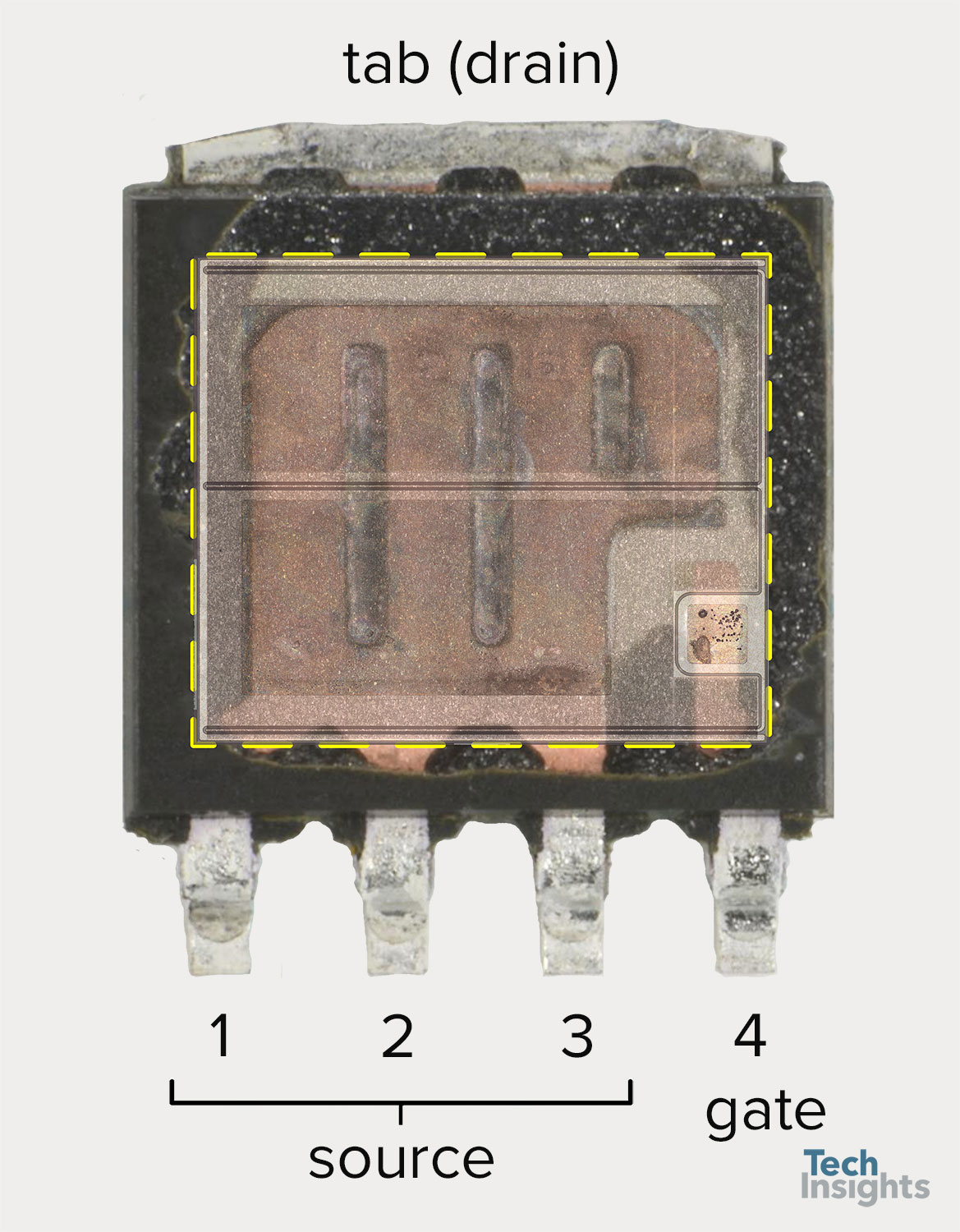
Figure 5. Nexperia PSMN3R9 jet-etch of package with copper clip source connection visible.
Summary
Although bespoke packages for wide bandgap devices such as GaN are still in their infancy it is a topic that is set to see intense development over the next decade. There are innovative solutions to shift the device terminals such as circuit-under-pad (CUP) structures and through-GaN trenches beginning to enter the market.
There is ongoing academic research into better thermal interface materials and die attach methods. Moving away from traditional soldering towards a sintered approach using silver is gaining momentum.
GaN has yet to find a foothold in high power module design, however in cutting edge SiC modules we are beginning to see specialised ceramic substrates such as Si3N4 and AlN being used for superior thermal dissipation.
Is there a solution in the die itself? Power Integrations takes the approach of using GaN-on-Sapphire wafers rather than GaN-on Si, while academic research has investigated more exotic approaches such as GaN grown on diamond.
Like all of power semiconductor there isn’t a one-size-fits -all approach and I think we will see more diversity and tailored solutions moving forward, it will be fascinating to watch!