Editorial: Nanometer Nonsense
Foundries Allow Customers to Lie About Manufacturing Process

Linley Gwennap
Many people lie now and then about their age or weight, but when companies lie, it can be seen as false advertising or at least brand dilution. This situation recently arose in the semiconductor market when both of the leading foundries allowed customers to claim they were using a 4nm process when, in fact, they were using 5nm technology. This situation makes everyone look bad, especially the foundries. It’s symptomatic of slowing transistor progress.
The problem started when Samsung, in a perennial race to beat TSMC to the next node, announced it would deliver production 4nm chips in late 2021, a year after it reached 5nm. TSMC had planned to take two years between its 5nm and 4nm nodes, delivering the latter in 2Q22, as Figure 1 shows. To avoid giving Samsung bragging rights, it decided to “pull in” its N4 node by two quarters, coincidentally matching its rival (see MPR, “Fewer Find 3nm Worth the Wait”). The first (and so far only) chip using N4 was MediaTek’s Dimensity 9000.
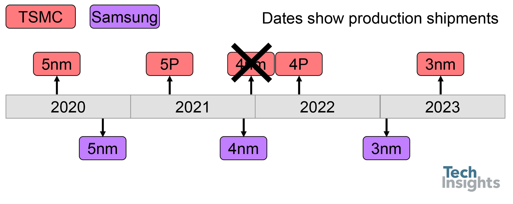
Figure 1: Revised foundry process roadmap. TSMC claimed to have delivered its 4nm node with late-2021 production, but it was just mislabeled 5nm technology.
Perhaps we should’ve been suspicious that TSMC could suddenly take six months out of its usual rigorous and time-consuming production-qualification cycle. But the jig was up when TechInsights analyzed the Dimensity 9000 and found the critical process dimensions were exactly the same as in TSMC’s earlier N5 products (see MPR, “Dimensity 9000 Now Available in Plus Size”). The foundry’s claim of 4nm production was a sham, as was MediaTek’s claim of having a 4nm processor.
Meanwhile in a Distant Galaxy…
In the meantime, Samsung’s smartphone unit was preparing to launch the Galaxy S22 and noticed that the company’s own Exynos 2200 is built in 4nm but Qualcomm’s Snapdragon 8 Gen 1, which appears in some S22 models, uses 5nm. To avoid customers lusting for one processor over the other, the companies decided to launch the 8 Gen 1 as a 4nm part. Because Samsung manufactures both, it created a new process called 4LPX that, like N4, serves only one product. After analyzing the Snapdragon chip, TechInsights found that 4LPX is physically no different than 5LPE.
Ironically, the only product using real 4nm technology has fared worse than the fake-4nm products. Samsung pushed too hard to get its 4LPE process into production, resulting in high defect rates and poor power efficiency for the Exynos 2200—particularly in its new graphics engine (see MPR, “Exynos 2200 First With AMD GPU”). Having limited supplies of the Exynos chip, the phone maker installed the Snapdragon processor in most Galaxy S22 models.
These production woes helped convince Qualcomm to jump ship, creating a new version of its flagship processor, called the Snapdragon 8+ Gen 1, for TSMC’s newer N4P, which we believe to be an actual 4nm technology. The new Snapdragon was the first announced N4P product, although we expect Apple’s A16 uses N4P as well. Both chips are already in production and will appear in phones around September.
TSMC usually gives Apple one or two quarters of exclusive access to its newest manufacturing technologies. It’s surprising to see Qualcomm on the list of initial customers, particularly since Snapdragon-based smartphones compete directly against Apple’s iPhones. TSMC apparently was willing to break Apple’s exclusivity in order to take away a major design from Samsung. (Qualcomm uses TSMC for many other products but has relied on Samsung to build its past few flagship processors.)
The Truth Is Hard to Handle
Why are the foundries suddenly lying about their transistor progress? It’s easier than admitting that progress has gotten mighty thin. The difference between a fake 4nm process and a “real” 4nm process is a mere 5% optical shrink (10% area reduction). Even that small advance broke Samsung’s yield model and took TSMC two years to complete. Both foundries expect to achieve volume production of 3nm next year, but their struggles with 4nm fail to inspire confidence.
Given the longer time between nodes, foundries may improve speed, power, or yield (which ultimately amount to the same thing) while waiting for the next node. While 4LPX has the same dimensions as 5LPE, for example, it may offer some other benefits that justify a new name. But without any improvement in transistor density, the name should have been 5LPX to indicate that the process is still a member of the 5nm node. Most people use the shorthand of 5nm or 4nm instead of the full process name, so the number is still important.
Although it gets them out of a short-term jam, faking new nodes is bad for the foundries. Touting a false 4nm milestone and allowing customers to advertise it dilutes the value of the foundries’ branding. If 4nm isn’t 4nm, do node names even matter? Why pay extra for 4nm technology if you can just rename an older process?
Foundries haven’t kept a strict correlation between node numbers and transistor density for some time (see MPR, “Editorial: Nanometer Madness”). But at least when they assigned a smaller nanometer figure, it indicated some density progress. To blatantly relabel a 5nm process as 4nm removes the last shred of meaning from node numbering. So when a foundry says it has reached the next level, don’t count on it until the teardown confirms it. The same holds true for chip vendors touting their access to new manufacturing technology. As Moore’s Law staggers to an end, we’re left with lies, damned lies, and node names.