MicroBT Whatsminer M56S++ Transistor Characterization
Share This Post
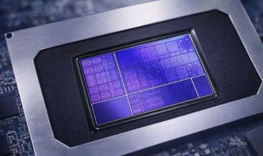
This report presents key DC electrical characteristics for logic NMOS and PMOS transistors located in the core region of the crypto-miner cryptocurrency ASIC die (KF1978) found inside the MicroBT KF1978E component. The MicroBT Whatsminer M56S++cryptocurrency miner contains 320 KF1978E components mounted on the main printed circuit board. The KF1978 die was manufactured on 300 mm wafers using Samsung’s SF3E process, formerly known as 3GAE, Samsung’s early version of their 3 nm process. The MicroBT KF1978 is the first high-volume device manufactured using gate-all-around (GAA) CMOS process.
The GAA transistors are formed using Samsung’s proprietary Multi-Bridge-Channel FET (MBCFETTM) technology. The KF1978 die back-end of line (BEOL) features 15 levels of metallization including 14 Cu metals and a top Al terminal layer. The Samsung KF1978 die is packaged in a Flip chip with DFN-like footprint. Logic transistors from the core region of the KF1978 die were characterized at 30 ºC in a scanning electron microscope(SEM) environment using a Kleindiek Nanotechnik prober and a Keithley 4200-SCS semiconductor characterization system.


