YMTC 128L Xtacking 2.0 for SSD!
Finally, they might catch up with Samsung, SK hynix, and KIOXIA

Dr. Jeongdong Choe
September 23, 2021
TechInsights just found and quickly reviewed YMTC 128L TLC die removed from Asgard Memory (Powev Electronic Technology Co.) PCIe4.0 NVMe1.4 AN4 1TB SSD with a double-sided PCB layout. Depending on the SSD products, package markings of the YMTC 128L 3D NAND Flash devices are different, for example, YMN09TC1B1HC6C (Date code: 2021 9W) or POWEV PYT02TV4IA1-X4PWA (Date code: 2021 31W).
The devices have the new 3D NAND 128L Xtacking 2.0 dies fabricated from Yangtze Memory Technologies Co (YMTC), top Chinese memory chip maker. The 1 TB SSD has four 256 GB NAND (YMTC) devices together with two 512MB DDR4 (Nanya) devices. Four NAND dies are assembled in a device, which means it’s a 512 Gb die.
Figure 1 shows package markings, Figure 2 shows NAND die markings (CDT1B), and Figure 3 shows CMOS die markings (CDT1A or CDT1B) of YMTC 512 Gb 128L Xtacking 2.0 3D TLC NAND chip. For the reference, YMTC 64L Xtacking 1.0 TLC die has slightly different die markings for NAND die (Y01-08 BCT1B) and CMOS peripheral die (Y01A08 BCT1B).
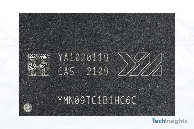
Figure 1. YMTC 128L Xtacking 2.0 package markings
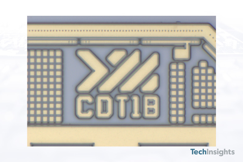
Figure 2. YMTC 128L Xtacking 2.0 512Gb NAND die markings
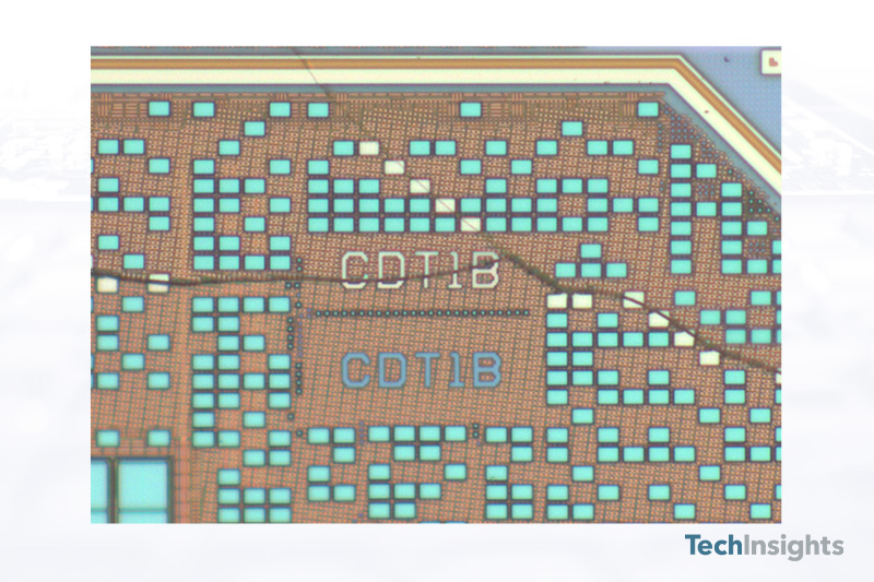
Figure 3. YMTC 128L Xtacking 2.0 peripheral CMOS die markings
YMTC’s 128-Layer Process Achieves a New Industry Leading Standard for Capacity, Bit Density, & I/O Speed
It seems quite meaningful as Samsung 176L V-NAND and SK hynix 176L 4D PUC NAND SSDs haven’t been found on the commercial market yet. YMTC 512Gb 128L Xtacking 2.0 TLC die size measures 60.42 mm2. Bit density increases to 8.48 Gb/mm2, 92% higher than the Xtacking 1.0 die (256Gb). Since YMTC Xtacking hybrid bonding technology uses two wafers to integrate the 3D NAND device, we can find two dies, one for NAND array die and another one for CMOS peripheral die.
Figure 4 shows NAND die floorplan and Figure 5 shows CMOS peripheral die floorplan of YMTC 128L Xtacking 2.0 chip. The Xtacking architecture is designed to allow YMTC to get ultra-fast I/O while maximizing the density of their memory arrays, for example, 7500 MB/s read and 5500 MB/s write for the SSD. The die has four-plane design and all the CMOS peripheral circuitries such as page buffers, column decoders, charge pumps, global datapath and voltage generators/selectors are placed on the logic die under the 3D NAND cell array die.
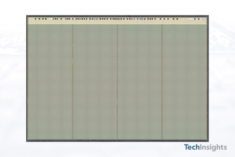
Figure 4. YMTC 128L Xtacking 2.0 NAND Die Floorplan
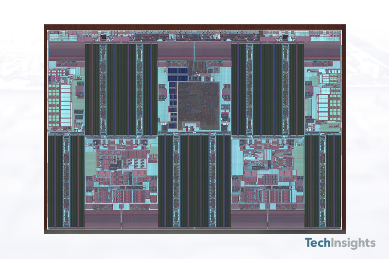
Figure 5. YMTC 128L Xtacking 2.0 Peripheral CMOS Die Floorplan
YMTC 128L Xtacking 2.0 Imaging, Specifications & Cell Structure
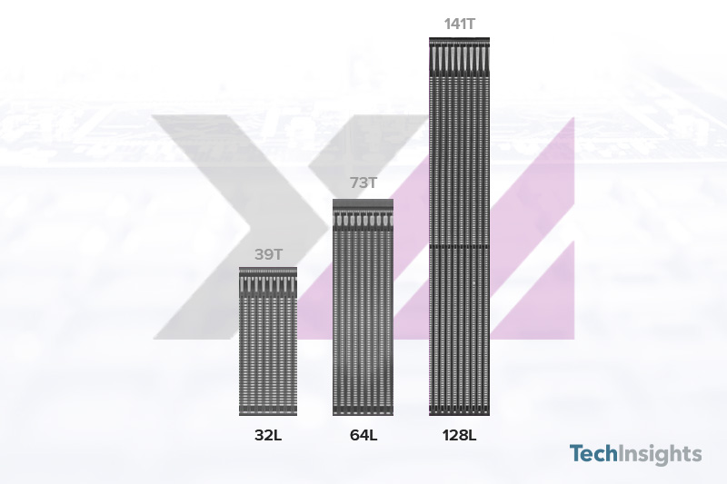
Figure 6. YMTC 3D NAND cell structure from 32L through 128L (x-section SEM images in WL direction)
YMTC 128L Xtacking 2.0 cell architecture consists of two decks connected through deck-interface buffer layer which is the same process with KIOXIA 112L BiCS 3D NAND structure. Cell size, CSL pitch, and 9-hole VC layouts keep the same design and dimension (horizontal/vertical WL and BL pitches) with previous 64L Xtacking 1.0 cell. Total number of gates is 141 (141T) including selectors and dummy WLs for the TLC operation.
Figure 6 shows YMTC 3D NAND cell structure in WL direction, and total number of gates annotated for 32L (T-CAT with 39T), 64L (Xtacking 1.0 with 73T), and 128L (Xtacking 2.0 with 141T).
The upper deck has 72 tungsten gates, while the lower deck consists of 69 gates. The total number of metal layers including BEOL Al, NAND die, and peripheral logic die counts 10, which means two Cu metal layers are added into the peripheral logic die comparing with 64L Xtacking 1.0 process integration. Channel VC hole height increases doubled, 8.49 µm. Table 1 shows a comparison of YMTC 3D NAND devices; Gen1 (32L), Gen2 (64L, Xtacking 1.0), and Gen3 (128L, Xtacking 2.0).
| Device | YMTC 3D NAND Gen1 (32L) | YMTC 3D NAND Gen2 (64L) | YMTC 3D NAND Gen3 (128L) |
|---|---|---|---|
| Parent Product Example | 32GB Secure USB | Gloway YCT512GS3-S7 Pro SSD 512GB |
Asgard PCIe4.0 NVMe1.4 AN4 1TB SSD |
| Package Markings | YMEC6A1MA3A2C1 | YMN08TB1B1HUB1B | YMN09TC1B1H6C |
| Die Markings | 98081A | BCT1B | CDT1B |
| MLC Operation | MLC | TLC | TLC |
| Architecture | T-CAT | Xtacking | Xtacking |
| Number of Dice/Device | 4 | 4 | 4 |
| Memory (/die) | 64 Gb | 256 Gb | 512 Gb |
| Die Size | 76.30 mm2 | 57.96 mm2 | 60.42 mm2 |
| Memory Density | 0.84 mm2 | 4.42 mm2 | 8.48 mm2 |
| Planes | 1 | 2 | 4 |
| Number of Decks | 1 | 1 | 2 |
| Number of Total Gates | 39T | 73T | 141T (69 + 72) |
| Number of Metals | 3 | 8 | 10 |
| Channel Hole Height | 2.74 µm2 | 4.14 µm2 | 8.49 µm2 |
Table 1. A comparison of YMTC 3D NAND devices; Gen1 (32L), Gen2 (64L, Xtacking 1.0), and Gen3 (128L, Xtacking 2.0)
By comparison with existing 128L 512 Gb 3D TLC NAND products from Samsung (V-NAND), Micron (CTF CuA), and SK hynix (4D PUC), die size is smaller than others, which makes it the highest bit density. Four-plane die floorplan and two-deck array structure are the same with Micron and SK hynix, however the number of selectors and dummy WLs per string is thirteen which is smaller than Micron and SK hynix (147T for both). Due to their Xtacking hybrid bonding method, the number of metal layers used is much higher than that of other products. Table 2 shows a comparison of 128L 512 Gb 3D TLC NAND products including YMTC 128L Xtacking 2.0 3D NAND just released.
| Device | YMTC 128L Xtacking | Samsung 128L V-NAND | Micron 128L CuA CTF | SK hynix 128L 4D PUC |
|---|---|---|---|---|
| Parent Product (Example) | Asgard PCIe4.0 NVMe1.4 AN4 1TB SSD |
Samsung EVO 870 1TB | Micron Crucial BX500 2.5 SSD 480GB |
SK hynix Gold P31 SSD 1TB |
| Package Markings | YMN09TC1B1H6C | K9DVGY8J5B-DCK0 | OYD2D NW987 | H25T2TB88E |
| Die Markings | CDT1B | K9AHGD8J0B | B37R | H25TFB0 |
| MLC Operation | TLC | TLC | TLC | TLC |
| Architecture | Xtacking | V-NAND | CTF CuA | 4D PUC |
| Number of Dice/Device | 4 | 16 | 2 | 8 |
| Memory (/die) | 512 Gb | 512 Gb | 512 Gb | 512 Gb |
| Die Size | 60.42 mm2 | 74.09 mm2 | 66.02 mm2 | 63.00 mm2 |
| Memory Density | 8.48 mm2 | 6.91 mm2 | 7.76 mm2 | 8.13 mm2 |
| Planes | 4 | 4 | 4 | 4 |
| Number of Decks | 2 | 1 | 2 | 2 |
| Number of Total Gates | 141T (69 + 72) |
136T | 147T (73 + 74) |
147T (77 + 70) |
| Number of Metals | 10 | 4 | 6 | 5 |
| Channel Hole Height | 8.49 µm2 | 6.23 µm2 | 8.42 µm2 | 7.53 µm2 |
Table 2. A comparison of 128L 512 Gb 3D NAND devices from YMTC, Samsung, Micron, and SK hynix
Dr. Jeongdong Choe has added YMTC 128L Xtacking 2.0 3D NAND onto 3D NAND 1GB Area Trends. Upcoming 162L and 176L devices are also predicted and added on the chart. It looks good enough to compete with other products from 3D NAND scaling viewpoint. It seems like YMTC has caught up with other frontrunners considerably.
Find content like this and more in the TechInsights Platform. Sign-up for free today.


