
Micron D1α, '14 nm'! The Most Advanced Node Ever on DRAM!
D1α! It’s 14 nm! After a quick view on Micron D1α die (die markings: Z41C) and cell design, it’s the most advanced technology node ever on DRAM. Further, it’s the first sub-15nm cell integrated DRAM product. Micron Z41C die removed from MT40A1G8SA-062E:R (FBGA Code: D8BPJ) is the most advanced 8 Gb DDR4-3200 (data rate = 3200 MT/s) SDRAM with Micron’s D1α technology applied. Micron described it as 40% improvement in density vs. D1z with ~10% driven by design efficiency.
TechInsights' Memory experts agree that the Micron D1α (1-alpha), '14 nm' show expansive system design applications such as:
- Advanced Mobile Platforms
- Enterprise Servers
- Client Systems
- Networking Infrastructure
- Storage Connectivity
- Artificial Intelligence & Machine Learning
Micron's D1α DRAM Products Use ArF-i Based Lithography Without EUVL Photomask Applied
Although D1y and D1z DRAM DDR4/LPDDR4/LPDDR5 products are major on market, Micron successfully developed and started shipping D1α DRAM chips since 4Q2020 (Figure 1). Micron D1α process integration technology and design/performance have been attracting a lot of public attention because D1α generation would be the first sub-15nm cell design. Further, Micron’s D1α DRAM products use ArF-i based lithography without EUVL photomask applied, which is quite different from Samsung’s EUVL strategy on DRAM scaling.
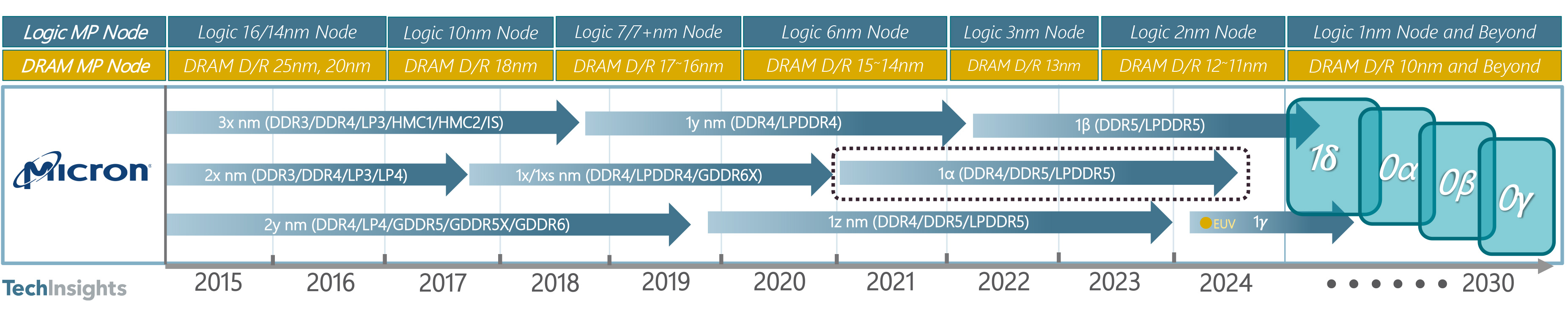
Figure 1. Micron DRAM technology roadmap. Micron extends D1α volume production in 2021.
D1α DRAM Device Analysis & Competitive Specifications
Given the die capacity and die size (25.41 mm2), bit density is 0.315 Gb/mm2 which is industry's highest DRAM density up to date. Previous D1z DDR4 DRAM dies from industry have 0.299 Gb/mm2 (Samsung 8 Gb Non-EUVL D1z DDR4), 0.247 Gb/mm2 (Micron 16 Gb D1z DDR4), and 0.296 Gb/mm2 (SK Hynix 16 Gb D1z DDR4 C-die), which means Micron increases ~28% bit density from D1z.
From cell size trend as shown in Figure 2, DRAM cell size has scaled down on and on. Blue square shows Samsung, and gray circle shows Micron’s DRAM cell size. Until D1x generation, between Samsung and Micron, they had a little technology gap, always Samsung had led Micron for each generation. However, for D1y generation, the gap had more narrowed, and all the big three DRAM companies showed the same cell size for D1z generation. Recently, Micron successfully caught up with Samsung for D1z generation, and further Micron already introduced their new and advanced D1α generation products on the market this year. We found and quick viewed Micron D1α generation cell design, and cell size measured 1,672 nm2, which is the smallest cell size on DRAM up to date.
Figure 3 shows Micron DRAM cell D/R shrink ratio trend from D2x through D1α. Micron kept 0.87 for many years, however for Micron D1z and D1α, the shrink factors increase to 0.92 and 0.9 for each. It’s getting harder to shrink cell size on DRAM.
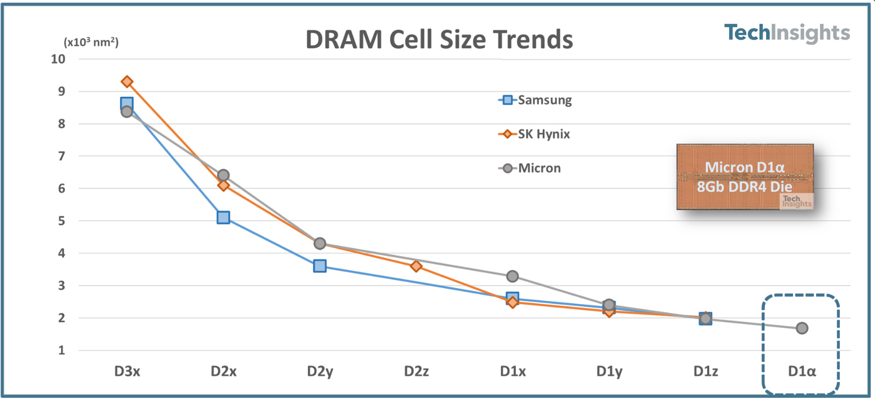
Figure 2. DRAM cell size trends from three big players; Samsung, SK Hynix and Micron, D3x through D1α
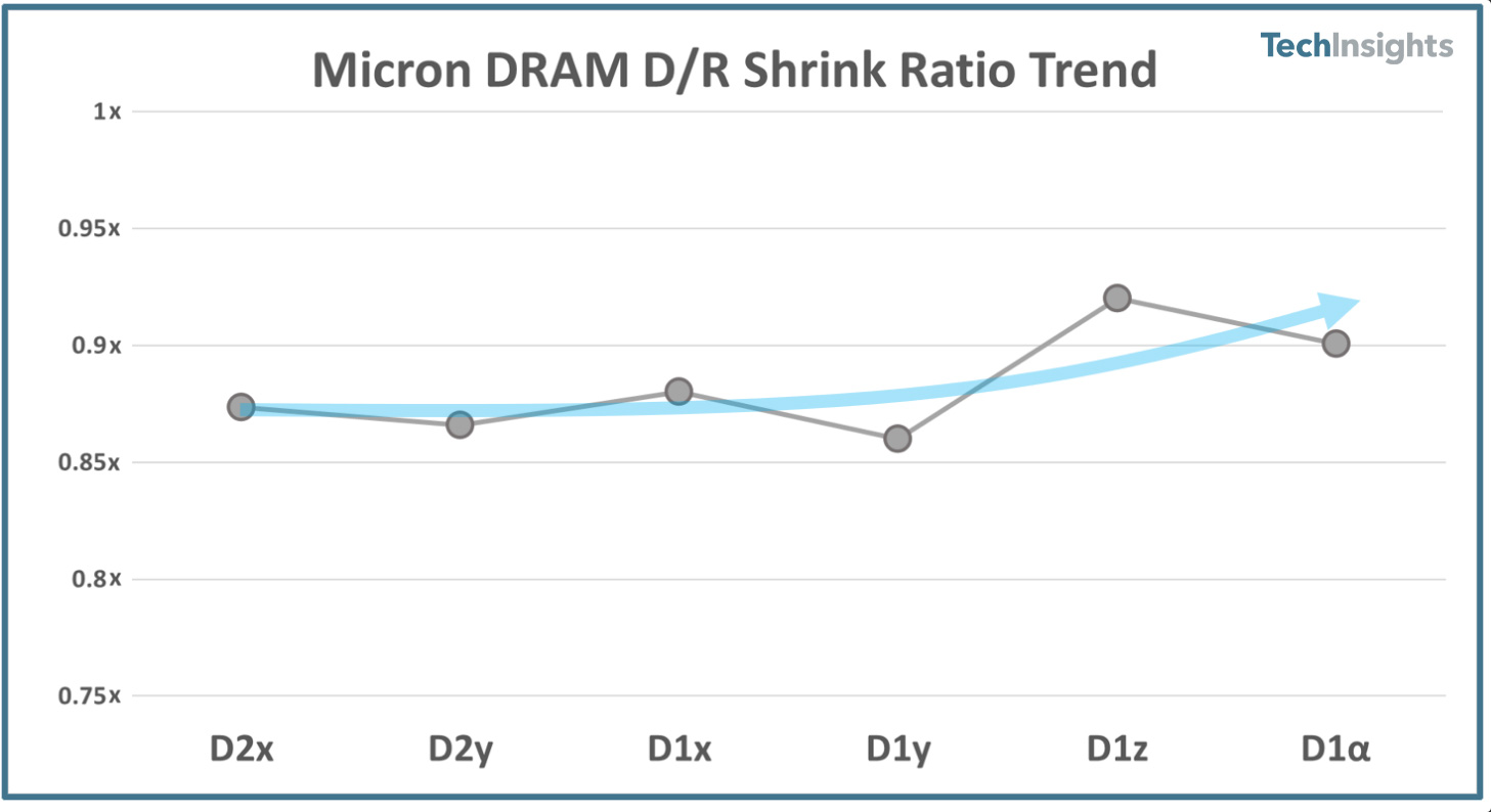
Figure 3. Micron DRAM cell shrink ratio trend, D2x through D1α
Tags: Micron D1α DRAM Memory
Find content like this and more in the TechInsights Platform. Sign-up for free today.