Micron B47R 3D CTF CuA NAND Die, the World’s First 176L (195T)!
Micron’s 176L 3D NAND is the world’s first 176L 3D NAND Flash memory. TechInsights just found the 512Gb 176L die (B47R die markings) and quickly viewed its process, structure, and die design. Micron 176L 3D NAND is one of the most groundbreaking technologies to date, and it is especially for the storage application such as data center, 5G, AI, cloud, intelligent edge, and mobile devices. Micron already announced its performance improvement, for example, read latency and write latency improved by more than 35% from 96L FG CuA, and over 25% from 128L CTF CuA.
TechInsights' NAND & DRAM Memory experts agree that the 176-layer NAND Universal Flash Storage (UFS ) shows expansive system design applications such as:
- High-End Flagship Phones
- High Capacity, Small Form Factors Required In Mobile Devices
- Professional Workstations
- Ultrathin Notebook Computers
- 5G Network Speeds
TechInsights' Reverse-Engineering Labs Architectural Findings on the 176-Layer NAND Universal Flash Storage (UFS) 3.1 Mobile Solution
We tore-down Micron 3400 1TB SSD (PCIe Gen-4 cSSD NVMe 1.4) and got the MT29F4T08EQLEEG8-QB: E (FBGA Code: NY124). Two 512Gb devices are packaged on the board for 1TB SSD. The 3400 SSD uses Micron’s latest in-house SSD controller, DM02A1, which is different from previous 2300 SSD (96L) and Crucial P5’s DM01B2 controller.
Micron 176-Layer NAND Universal Flash Storage Die-Level Imaging and Specifications
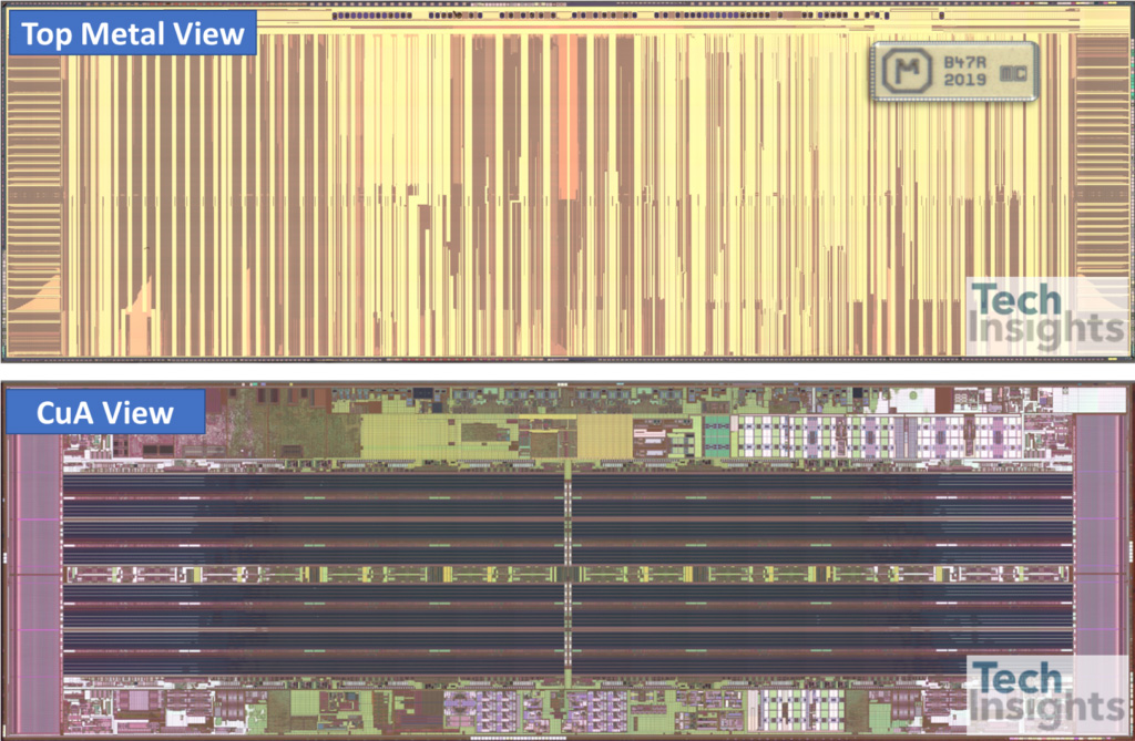
Figure 1. Micron 176L 512Gb TLC die images; top metal viewed and CuA viewed (die markings added)
Figure 1 shows a top metal viewed die, a CMOS circuitry viewed die, and B47R die markings. In comparison with previous 128L CTF CuA 512Gb B37R TLC die, die size decreased by 25% due to higher cell density, increased 3D NAND cell numbers, and page buffer/wordline switches design scaling effectively.
The 176L 3D NAND is the 2nd generation CTF structure for Micron. The NAND cell array height (the height from source-side selector to BL, for comparison) is now more than 11 µm. Total number of gates including selectors (STs) and dummy word lines (DWLs) per vertical NAND string is 195, 195T so called, which is the highest number ever on 3D NAND (Figure 2). They keep double stack architecture, replacement-gate process, charger trap nitride (CTN), and CMOS-under-Array (CuA) techniques.
Feature Comparisons of 3D NAND Market Leaders and Devices
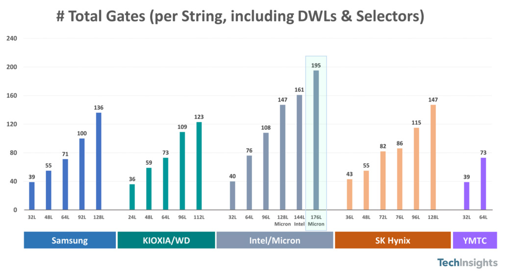
Figure 2. A comparison of total number of gates for 3D NAND players and devices
Bit density reached to 10.273 Gb/mm2 for 512Gb TLC die by substantially shrinking the die size compared with previous 128L 512Gb TLC die (B37R die markings, 7.755 Gb/mm2, please refer to the TechStream Memory blog; https://app.techinsights.com/blog-post/2070 for more details). It’s the world’s first TLC Micron 512Gb TLC NAND die size.
Micron 128L Vs. New 176L Cell Structure and Bit Density
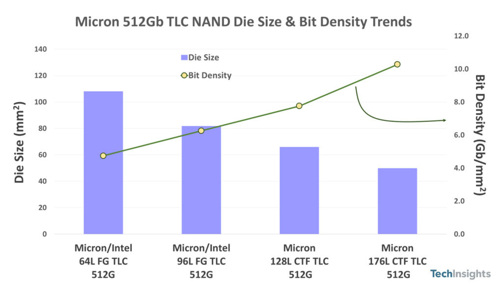
Figure 3. Micron 512Gb TLC NAND die size and bit density trends, up to 176L
In comparison with Micron 128L, the new 176L cell structure consists of two decks with 88 WLs for each. Interconnection metals and contacts/vias for BEOL and CuA are the same with 128L, while vertical channel (VC) hole height increased to 10.6 µm. 3D NAND unit cell size in WL and BL directions keeps 0.02 µm2, while unit cell volume slightly decreased to 1.12 x 10⁻⁴ µm3 due to a smaller gate pitch (Table 1).
| Device | Micron 128L 512Gb | Micron 176L 512Gb |
|---|---|---|
| Parent Product Ex. | Crucial BX500 SSD (2021) |
Micron 3400 1TB SSD (2021) |
| Process (Storage) | CFT (CTN) | CFT (CTN) |
| Operation | TLC | TLC |
| Die Markings | B37R | B47R |
| Die Size | 66.02 mm2 | 49.84 mm2 |
| Bit Density | 7.76 Gb/mm2 | 10.27 Gb/mm2 |
| # Total Gates (Vertical) | 147T | 195T |
| # Active WLs | 128 | 176 |
| # Decks | 2 | 2 |
| # WLs Assigned | 64 + 64 | 88 + 88 |
| # Metals | 6 (4W, 1Cu, 1Al) | 6 (4W, 1Cu, 1Al) |
| CMOS Architecture | CuA | CuA |
| Unit Cell Size | 0.020 µm2 | 0.020 µm2 |
| Unit Cell Volume | 1.14 x 104 µm3 | 1.12 x 104 µm3 |
| VC Height (including Selectors) |
8.5 µm | 10.6 µm |
Table 1. A comparison table of device features, Micron 512Gb 128L vs. 176L
As the number of cell gates increase beyond 150L, we expect a lot of challenges are there, for example, alternative layers stacking (mold layers), WL staircase optimization, vertical channel hole HAR etching and ALD layer process, ONO cut, deck misalign, sacrificial layer removal, replacement gate fill, CSL trench profile, wafer warpage, and related process uniformity. We’ll look through and track down them all on the successfully commercialized 176L devices.
Tags: Micron 176L NAND Memory
Find content like this and more in the TechInsights Platform. Sign-up for free today.


