Intel's 2nd Generation XPoint Memory - Will it be worth the long wait ahead?
In 2017, TechInsights analyzed the details on Intel 1st gen. XPoint Memory (OptaneTM Memory 16GB, MEMPEK1W016GA) including structure, materials, process, design, and circuit as well. Since then, we’ve been waiting for the 2nd gen. XPoint Memory for many years. 3D XPoint non-volatile memory technology was introduced in 2015, and products started shipping from 2017. Micron’s strategy was providing data center customers such as Intel with persistent memory technology for cloud-native infrastructure. The initial value proposition was higher density, cheaper DRAM, and faster NAND. However, Micron decided to exit 3D XPoint non-volatile memory market, instead focusing its data center efforts on the emerging Compute Express Link (CXL) interface. As Micron Technology just gave it up recently although they have 1st XPoint Memory products (X100 SSDs) for limited customers, Intel is now the only company on this.
Intel has announced three new memory products in the Optane family with 2nd gen. 3D XPoint Memory last December. The 2nd gen. XPoint Memory has four-layer Phase Change Memory (PCM) structure for 256Gb die. The Optane P5800X is said to be the fastest enterprise SSD with PCIe NVMe 4.0 x4 on the market.
There is also a new hybrid SSD with NAND and 3DXP as well as a new generation of Optane DIMM with Crow Pass. The Optane Memory H20, an SSD that combines a large part of 3D NAND with a small part of 3D XPoint, appears under the code name Pyramid Glacier. The introduction of the Intel Optane H20 SSD is scheduled for the second quarter of 2021. The third generation of the Optane Persistent Memory, also known as Optane DIMM, is now on the agenda with Crow Pass, which is only due to appear with the upcoming Sapphire Rapids server platform, which is not expected until the end of 2021 at the earliest.
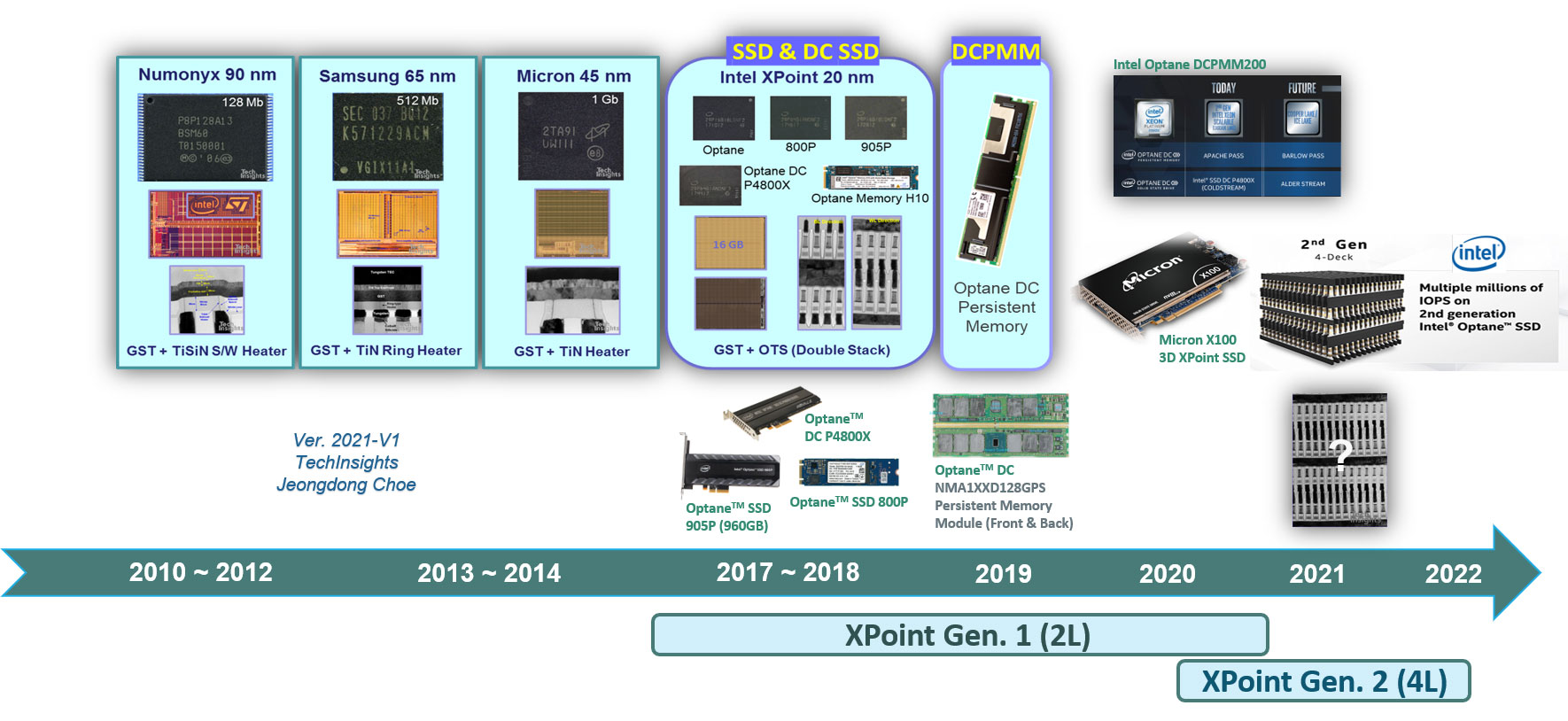
Figure 1. History of XPoint and PCM devices revealed on the market
In the meantime, we’d better briefly recall and review the 1st gen. XPoint Memory technology, especially on structure, materials, and die/block design. Figure 1 shows XPoint/PCM history. The 1st gen. XPoint Memory die has 128Gb (16GB) die density and two-layer PCM structure. It has been used many of Intel SSD products such as Optane, 800P, 900P, DC P4800X, H10 and DCPMM.
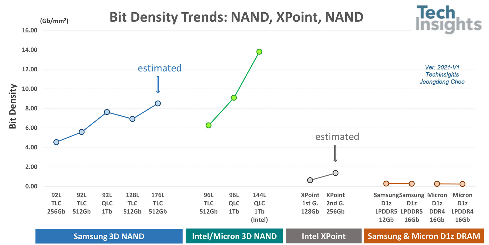
Figure 2. A comparison of bit density; 3D NAND from Samsung, Intel and Micron, Intel XPoint, D1z DRAM from Samsung and Micron
When it comes to memory bit density, Intel Optane XPoint 1st gen. has 0.62 Gb/mm2, higher than DRAM dies (average bit density 0.23~0.27 Gb/mm2 for D1z node DRAM products), while quite lower than currently commercialized 128L or 144L 3D NAND products, for example, Samsung 128L 512Gb TLC (6.91 Gb/mm2), SK Hynix 128L 512Gb TLC (8.11 Gb/mm2) and Intel 144L QLC (12.86 Gb/mm2). Figure 2 shows a comparison of bit density; 3D NAND from Samsung, Intel and Micron, Intel XPoint, D1z DRAM from Samsung and Micron. We estimated and added up-coming Samsung 176L 512Gb TLC 3D NAND and Intel 2nd gen. XPoint Memory 256Gb dies into the graph. If the 2nd gen. XPoint Memory 256Gb die has the same die size and well optimize the peripheral design, it increases to around 1.36 Gb/mm2, which is however still in a range of N1y or N1z 2D NAND. For higher density Storage Class Memory (SCM) application, more innovative and new architecture concept would be needed.
Intel XPoint cell array structure and peripheral design use a concept of CMOS under Array (CuA) which is also used for Intel/Micron 3D NAND building. By using CuA-type integration, Intel and Micron’s 3D NAND memory array efficiency is quite higher (~85%) than non-CuA products (60~70%). Likewise, memory efficiency for XPoint memory die is more than 90% since the storage elements in XPoint memory array are located between metal 4 and metal 5. In other words, all the CMOS circuits such as drivers, decoders, BL access, local data and address control are placed under the memory elements, which is similar with CuA architecture for 3D NAND. Peripheral die designed with a tile-type floorplan which is the same with Intel/Micron CuA 3D NAND dies. 16,384 tiles per die means 7.81 Mb/tile density, and 2,150 BLs and 2,150 WLs per tile including dummy WLs and BLs are allotted.
A double layered storage/selector structure was used for the 1st gen. XPoint Memory. For the storage elements, many candidates such as phase change materials, resistive oxide cells, conductive bridge cells and MRAM cells have been proposed and developed. Among them, the 1st gen. XPoint Memory adopted a chalcogenide-based phase change material, GST (Ge-Sb-Te) alloy layer. A 20nm double patterning technology (DPT) used for BL and WL lithography/etching process. Effectively, 2F2 cell designed on the XPoint Memory cell array.
For the selector elements, many of switching devices such as a transistor-type (BJT or FET), diode-type and ovonic threshold switch can be used. Intel 1stgen. XPoint Memory uses another chalcogenide-based alloy with arsenic (As) doped, which is different from GST alloy PCM layer. The selector material Intel used is an ovonic threshold switch (OTS) material. The overall structure consists of a double stacked memory layers and OTS selector elements along bitline and wordline. OTS selectors are not extended over middle electrode or bottom electrode.
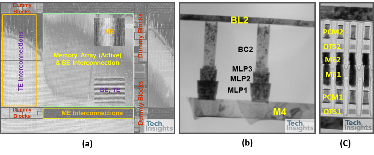
Figure 3: Images describing some issues on process and design; (a) Dummy blocks and interconnection area near an active array, (b) multi-pads on M4, and (c) PCM/OST cell structure with ME1 tungsten layer separated from ME2
Some of issues to be improved on process and design were there, for example, array and peripheral area mismatch, throughput/cost, WL/BL interconnection area penalty, and cell scaling. Figure 4 shows some images describing the issues including (a) dummy blocks and interconnection area near active array, (b) multi-pads on M4, and (c) PCM/OST cell structure with ME2 tungsten process separated from ME1. Peripheral area is not well matched to the XPoint cell array area, which causes a lot of dummy cell blocks added between the active cell blocks. Due to the area penalty, cell area efficiency decreased to 57.8% although they use CuA structure. Three landing pads are used under WL, BL1 and BL2 contacts to connect with M4 layer on cell XPoint array, which may cause higher Rc and increase cost. Middle electrode (ME) layer consists of two separated W layers, ME1 and ME2, which means additional photolithography, etching and CMP processes are needed.
Why are we patiently waiting for the 2nd gen. XPoint Memory?
We expect many of the issues would be solved and improved from Intel for the 2nd gen. XPoint Memory products. We’re looking forward to finding how Intel update the XPoint technology.
Dr. Jeongdong Choe, Senior Technical Fellow
Dr. Jeongdong Choe is a Senior Technical Fellow at TechInsights. He has nearly 30 years of experience in the semiconductor industry, R&D and reverse engineering on DRAM, NAND/NOR FLASH, SRAM/Logic and emerging memory. He worked for SK Hynix and Samsung Electronics for over 20 years. He joined TechInsights and has been focusing on technology analysis on semiconductor process, device and architecture. He has written many articles on memory technology including DRAM technology trend, 2D and 3D NAND process/device integration details, and Emerging memory such as STT-MRAM, XPoint, ReRAM and FeRAM design and architecture. He quarterly produces and updates a widely distributed memory roadmaps on DRAM, NAND and Emerging memory.
Want to read more?
TechInsights Memory subscribers already have access to exclusive content in the TechInsights Platform.
Interested in a subscription?
TechInsights offers subscriptions to the broadest range of analysis and expert commentary. Contact us to learn about our many subscription offerings.


