Here, we have the Intel 2nd gen. XPoint Memory die!
Finally, we’ve found the Intel XPointTM Memory 2nd generation die! We’ve quickly viewed the die removed from Intel OptaneTM SSD DC P5800X 400GB (Model: SSDPF21Q400GB) which consists of eight storage devices, package markings with 29P64B14MDSG1, and just confirmed on it, with 4-stack XPoint memory layers which is effectively 1F2 cell structure.
XPoint Emerging Memory Technology Specifications
Intel announced Optane SSD P5800X specifications, including form factor (U.2 and E1.S), interface (PCIe 4.0 1×4, 2×2, NVMe 1.3d), ASIC/CPU (Single-core 1.1 GHz ARM Cortex R7), Read/Write performance (7.4GB/s SR & SW, 1.5M IOPS R4KR & R4KW), and endurance (100 DWPD) at the end of last year, however it’s the first time to check out the new cell structure with 4-stack PCM/OTS integration.
TechInsights' Embedded and Emerging Memory subject matter experts agree that the Intel 2nd gen. XPoint Memory products show expansive system design applications such as:
- Data Centers
- Cloud Service
- Real-Time Computing
- 3D Printing
- 3D Modeling
Intel 2nd gen. XPoint Die Imaging
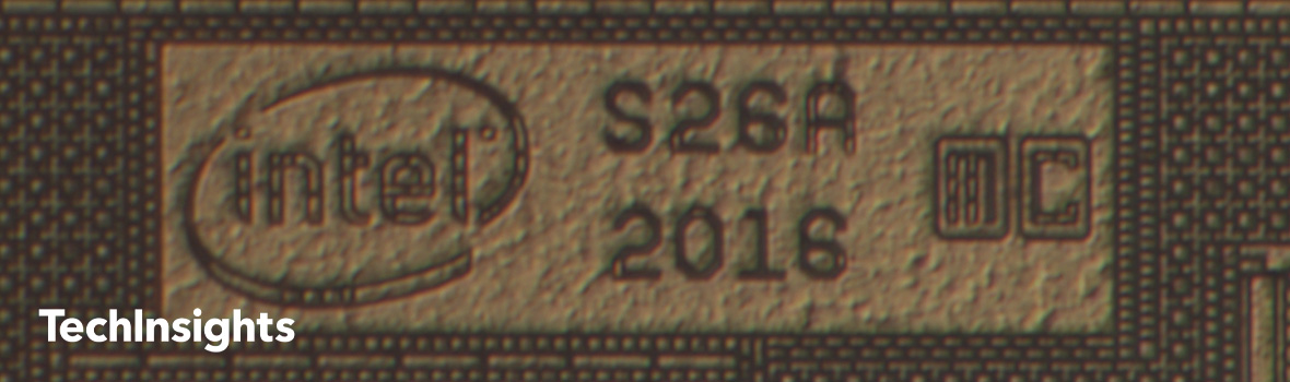
The 29P64B14MDSG1 is a two-die (two-chip) packaged 64GB device. Intel’s 1st gen. devices used for Optane 800P, 900P, DC P4800X, H10 and DCPMM have a one-chip 32GB package. The number of bond pads on the 2nd gen. die increased to 85. The die, S26A, shows 256 Gb/die, and 1.31 Gb/mm2 density which is doubled from the 1st gen. XPoint memory die. Figure 1 shows a 256Gb die (top-metal view) image and its die markings to compare with previous 128Gb die.
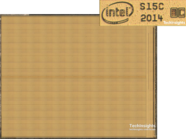
(a): Intel XPoint Memory 1
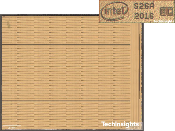
(b): Intel XPoint Memory 2
Figure 1. Die images (top-metal view) and die markings; Intel XPoint Memory (a) 1st gen. vs. (b) 2nd gen.
Intel 2nd gen. XPoint Memory Cell Structure
WL and BL pitches measure 40nm for each, which results in the same unit cell size, 0.0016µm2, with 1st generation. 4-stack PCM/OTS layer structure, effectively 1F2, is integrated on M4 layer, likely with a WL/BL/WL/BL/WL stack. The Ovonic Threshold Switching Selector (OTS) co-integrated with a PCM layer for the device, which is the same elements with XPoint 1st generation. Tungsten (W) WL and BL layers consist of multiple deposition, photolithography/etch and CMP processes, which may need more than eight masks for the 4-stack memory cell structure. Figure 2 shows a comparison of 2-stack (1st gen.) and 4-stack (2nd gen.) cell array structure (SEM x-section).
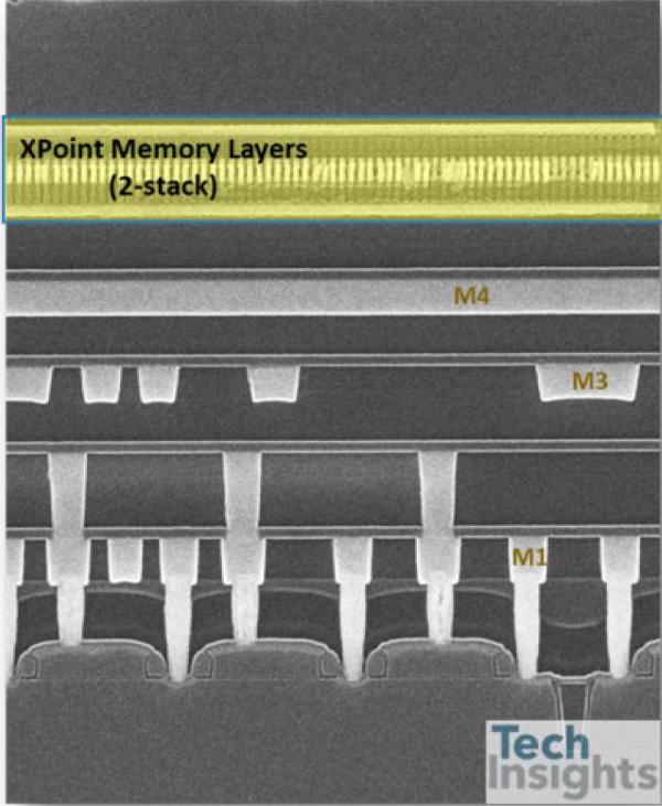
(a): Intel XPoint Memory 1st Gen. 2-Stack Cell Structure
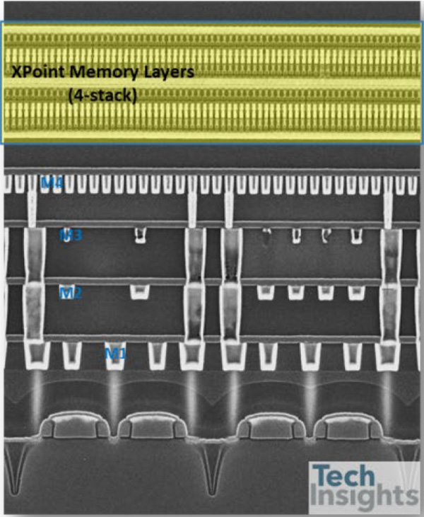
(b): Intel XPoint Memory 2nd Gen. 4-Stack Cell Structure
Figure 2. Intel XPoint Memory cell structure (SEM x-section); (a) 1st gen. 2-stack (2F2) vs. (b) 2nd gen. 4-stack (1F2)
Comparing 1st and 2nd Generation XPoint Memory
| XPoint Memory | 1st Generation | 2nd Generation |
|---|---|---|
| Parent Products (Ex.) | Intel Optane DC P4800X SSD |
Intel Optane DC P5800X SSD |
| Storage Device | 29P16B1BLDNF2 (single-die package) |
29P64B14MDSG1 (two-die package) |
| Process (Technology Node) | Intel XPoint 1st gen. (20 nm) | Intel XPoint 2nd gen. (20 nm) |
| Die Markings | 515C | 526A |
| Memory Capacity (Die) | 128 Gb | 256 Gb |
| Die Size | 206.5 mm2 | 195.6 mm2 |
| Bit Density | 0.62 Gb/mm2 | 1.31 Gb/mm2 |
| Unit Cell Size | 1,600 mm2 | 1,600 mm2 |
| # Metals (excluding WLs/BLs) | 5 | 5 |
| Cell Design (Effective) | 2F2 | 1F2 |
| Memory Structure | 2-stack array between M4 and M5 (WL/BL/WL) |
4-stack array between M4 and M5 (WL/BL/WL/BL/WL) |
| Pitch (WL, BL) | 40 nm, 40 nm | 40 nm, 40 nm |
| # Bond Pads (Die) | 81 | 85 |
| Memory Array Efficiency | 57.8% | 67.4% |
Table 1. A comparison table of Intel XPoint Memory devices; 1st Gen. vs. 2nd Gen.
Increasing Peripheral CMOS Memory Efficiency
From our quick analysis on the 2nd XPoint memory die design, memory array area efficiency increases to 67.4%, which means the XPoint cell array on peripheral CMOS (complementary metal oxide semiconductor) circuitry is well designed and optimized from the previous generation. Table 1 shows a detailed comparison of XPoint memory devices, Gen1 vs. Gen2.
Tags: Intel 2nd gen Emerging Memory
Find content like this and more in the TechInsights Platform. Sign-up for free today.


