Image Sensor Blog
iPhone 14 Pro's New Ambient Light Sensor – Inside the Package
John Scott Thomas
Treena Grevatt, PhD
January 25, 2023
Apple’s annual big reveal in September 2022 promised an iPhone 14 with “a re-engineered proximity sensor”, detecting light from behind the display to save additional space. This is the type of announcement the CIS subscription likes to hear about, and indeed our initial teardown analysis showed that Apple decided to change their approach to the proximity sensor.
Share This Post
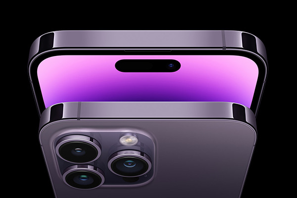
The front of the iPhone display has evolved from the conventional notch cut-out at the top of the phone (used for the selfie camera in Infra-Red (IR)devices) to a pill or “dynamic island” region (dynamic refers to the changing size and shape of the black oval as the function of the island changes; Figure 1 shows the island/pill in its quiescent state. This is the minimum size of the island).
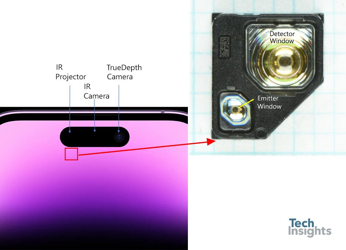
Figure 1: Apple iPhone 14 Pro front of display, location of proximity sensor under the active display is indicated. Orientation of the extracted sensor is preserved. TechInsights, 2022.
In Figure 1, the location of the proximity sensor relative to the island is shown, located beneath the active display, directly beneath the IR projector. On the right-hand side is the extracted proximity sensor, showing an emitting window and a larger detection window.
De-capping the sensor reveals three main functional devices as well as passive components mounted on two separate substrates as shown in Figure 2. Note that a metal cover that covered the Control IC has been removed to expose the IC.
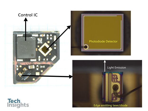
Figure 2: iPhone 14 Pro proximity sensor indicating the emitting device, detector, and control IC. TechInsights, 2022.
Consulting Figure 2, the optical components appear to be a basic photodiode detector and an edge-mounted laser diode. The laser diode is edge mounted on a large black slug presumably used as a heat sink. The control IC has package markings Y81/529IL/EDQCR, and the laser diode has die markings Y2/13/32.
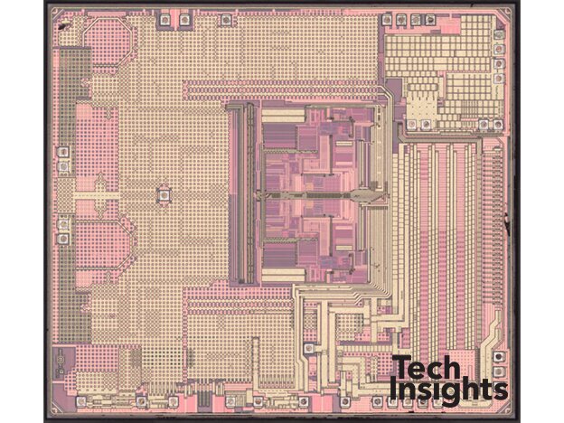
Figure 3: Control IC depotted, indicating an Analog Devices chip with die marking W30A. TechInsights, 2022.
Digging deeper, a depot of the control IC is shown in Figure 3. Die markings are ADI/21/W30A and the Analog Devices logo. A search through the Analog Devices catalog on these packages and die markings do not provide any further information. The layout suggests large drive circuits are present along with control digital circuitry, presumably used for time-of-flight measurement. Thirty-six bond pads (all wire bonded) are on the die, while the controller package has 30 (5 × 6) ball bonds.
This is a significant departure from previous iPhone proximity sensors. A search through the TechInsights teardown database shows that Apple has been using STMicroelectronics devices for the proximity sensor. There is no indication that STMicroelectronics is present in the iPhone 14 sensor. Looking at Table 1, this seat has been occupied by STMicroelectronics since at least the iPhone XS Max. Previous ST proximity sensors have used GaAs/AlGaAs Vertical Cavity Surface Emitting Lasers (VCSELs) mounted directly on a silicon chip containing Single Photon Avalanche Diode (SPAD)detectors (see Package Report PKG-2106-801 for a detailed analysis of this type of sensor). The new sensor has a simpler edge-mounted laser diode and simple photodetector.
| Smartphone | Proximity Sensor Manufacturer Release Date |
|---|---|
| iPhone XS MaxSTMicroelectronics | September,2018 |
| iPhone 11 Pro STMicroelectronics | September,2019 |
| iPhone 12 Pro STMicroelectronics | September,2020 |
| iPhone 13 Pro STMicroelectronics | September,2021 |
| iPhone 14 Pro Analog Devices(control IC) | September,2022 |
Table 1: Proximity Sensors in iPhone generations. TechInsights, 2022.
TechInsights performed further analysis on the laser diode to confirm the dimensions and materials of the laser.
The edge emitting laser diode is vertically mounted on a slug to direct light through the phone’s display. A single gold ball bond connects to a gold contact pad that contacts the p+ anode. The cathode connection is the backside of the device. The laser diode measures 270 µm wide with a cavity length of 430 µm. The die height is ~81 µm; this thickness will require careful handling during wafer thinning and bar cleave.
The topside view of the laser diode includes large nonelectrically connected pads that help protect the laser ridge from handling damage during the final stages of wafer thinning, bar cleave, and facet coating as well as acting as fiducials for any machine-vision test and assembly systems. Some facet coat overspray is observed wrapping onto the topside of the laser diode at each facet as color fringing. This overspray is desired to ensure that the facet is adequately coated and protected. The facet coating of the transmitting edge is designed to partially transmit light while the reflecting edge is adjusted for maximized optical reflection. Die singulation is performed along the die cleave channel to separate the devices.
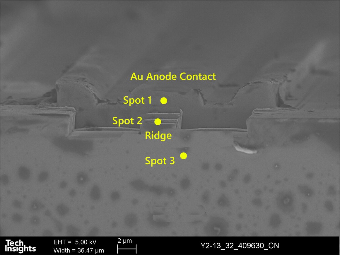
Figure 4: Reflecting Edge of Laser Diode Ridge, EDS locations indicated. TechInsights, 2022.
The back facet of the laser is shown in Figure 4. The laser ridge is 4.0 µm wide and 2.2 µm high. At first look this appears to be a Fabry-Perot gain-guided ridge waveguide laser structure. Performance demands for this application do not require sophisticated structures for narrow linewidths or high-speed modulation. The metallization is set back from the facet, which will help keep yields for bar cleave high, since any hazards due to metal overhang are removed. Maintaining low costs through high production yields is likely an important design driver for this type of component.
| EDS Point | Feature | Detected Elements |
|---|---|---|
| Spot 1 | Metal anode contact | Au |
| Spot 2 (surface) | Facet coating | Ta, Si, O |
| Spot 2 (bulk) | Ridge | In, P, As |
| Spot 3 | Substrate | In, P |
Table 2: SEM-EDS Analysis of Reflecting Facet and Ridge TechInsights, 2022.
SEM–EDS (Scanning Electron Microscope – Energy Dispersive X-Ray Spectroscopy) was performed on the materials as well to confirm the material system. Results are summarized in Table 2. The p-contact metallization is patterned and deposited in two stages. There is a 3-µm gold layer atop and slightly inset from the first metallization stack. We would expect a typical contact metal stack contacting to the p++ ridge cap semiconductor layer to be Ti/Pt/Au to provide a well-alloyed Ohmic contact whilst maintaining a barrier to prevent a reliability hazard ingress of Au into the semiconductor layers.
The gold contact (Figure 4, Spot 1) connects to the p+ anode through an etched p-contact via opening to the ridge (not shown, since this cross-section view is not through the contact region). The facet coating (Spot 2, surface) uses a thin film containing Tantalum, Silicon, and Oxygen to reflect the laser light. The ridge itself (Spot 2, bulk) contains Indium, Phosphorus and Arsenic. No Gallium was detected at that location in the ridge, but layers below the ridge do contain Gallium. The substrate (Spot 3) is Indium Phosphide.
As Apple reduces the display notch area to a pill, the proximity sensor is placed under the active display. A shift from the 905 nm wavelength to longer 1xxx nm is required to allow the light to transmit through the OLED display. A shift from a GaAs VCSEL device to the Indium Phosphide laser with an InGaAsP quaternary active region in the iPhone 14 achieves this. A simple ridge laser structure keeps the cost of the device low. The photodiode detector also uses Indium Phosphide.
The new iPhone 14 proximity sensor raises many questions. The new device appears to be simpler. Has costing been the main driver? Is the performance superior? Did Analog Devices manufacture the entire sensor module? What wavelength of light is being used? Is the display over the proximity sensor modified (for example, reduced pixel pitch) to allow light emission and detection? TechInsights Package report (PKG-2209-802) available to our subscribers, answers some of these questions.
Subscribers can also view the exploratory cross-section images (in the Package channel) for a deeper analysis and more EDS results.
Discover what the Image Sensor Package Channel offers our subscribers here.


