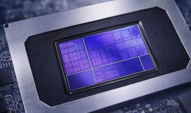
Intel PowerVia Bypasses Frontside Metal
At the recent VLSI Symposia, Intel presented three papers discussing PowerVia technology: one on the technology itself, another on the results from a test microprocessor, and a third looking at the possible evolution of PowerVia.

Dick James
A major challenge in semiconductor design is getting the power down to the transistors. Chips can have up to 18 levels of metal, needed to power the device and get signals in and out. This complex stack of metals forces power lines to be longer than ideal, increasing voltage droop and parasitic capacitances.
Separating the signal and power lines, to allow independent optimization of signal and power interconnect layers, would allow both to be shorter, reducing the voltage droop and parasitics and simplifying routing—the question is, how to do it?
The signal lines gain from lower resistance and capacitance, while the power lines have lower resistance. Intel plans to introduce PowerVia in its 20A generation, scheduled for production in late 2024.
At the VLSI Symposia in June, Intel presented three papers discussing the technique: one on the technology itself, another on the results from a test microprocessor, and a third looking at the possible evolution of PowerVia.
They claimed an IR droop reduction of ~30%, more than 5% improvement in frequency, and over 90% cell density thanks to the introduction of PowerVia.
Free Newsletter
Get the latest analysis of new developments in semiconductor market and research analysis.
Subscribers can view the full article in the TechInsights Platform.
You must be a subscriber to access the Manufacturing Analysis reports & services.
If you are not a subscriber, you should be! Enter your email below to contact us about access.


