Groundbreaking SenSWIR Sensor by Sony - IMX990/IMX991
Sony announced the IMX990 and IMX991 SenSWIR imagers in 2020, with a 1.34 MP and 0.34 MP resolution, respectively. By moving away from pixel-level bump bonds and taking advantage of greater miniaturization in Cu-Cu Direct Bond Interconnect (DBI), Sony was able to reduce the pixel size of the InGaAs/ROIC SWIR imagers down to 5.0 µm. This makes the IMX990/IMX991 the smallest pixel-pitch InGaAs-based SWIR image sensors commercially available on the market.
Sony Semiconductor Solutions Die-to-Wafer Hybridization Advanced Packaging Process
Additionally, Sony has developed a highly scalable Die-to-Wafer Hybridization process, with wafer-level hybrid bonding to help manufacture its new SWIR imagers. In Die-to-Wafer Hybridization, a handle wafer supports an array of pre-manufactured SWIR InGaAs Die so that hybrid bonding can take place much like conventional CMOS Image Sensors CIS-to-ISP wafer-level bonding.
This approach presents two advantages, the Cu-Cu DBI can help reduce the overall height of the Die while Die-to-Wafer hybridization can help reduce the per-Die cost, thereby facilitating greater utilization of Sony’s SWIR technology for a wide range of applications. Recently, TechInsights revealed the first detailed cross-sectional image of the 1.34MP.
TechInsights Image Sensor analysis shows the reason why the IMX990/IMX991 has improved VIS-IR response and is competitive in applications such as:
- industrial cameras
- inspection equipment
- material selection
- semiconductor inspection
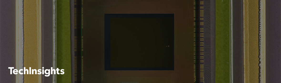
Sony IMX990 Die Photograph
The IMX990 optical Die photo is shown in Figure 1. The figure shows Die width and height to be about 12 mm and 10 mm respectively, giving a Die area of about 120 mm2. The InGaAs SWIR Die is the central blue/orange-colored region. It consists of the light shield (blue) covering Dark pixels, and the active imageable area (orange). The pixel structure in the SWIR imageable region appears homogeneous with no discernable features. The total SWIR area measures about 7.4 mm in width and 6.0 mm in height (or about 44.4 mm2). The imageable infrared-sensitive Photo Detection Area (PDA) measures about 6.7 mm in width and 5.3 mm in height (or 35.5 mm2). The diagonal of the active PDA region is about 8.3 mm and is consistent (within the measurement error) with the value of 8.2 mm reported by Sony for the IMX990.
The optical Die photo also shows the peripheral circuitry of the CMOS Read Out Integrated Circuit (ROIC) around the SWIR zone. The ROIC circuitry is visible because the Hybridization process of the InGaAs Die leaves an optically transparent dielectric “filler” around it.
Figures 2 (a) and 2 (b) further highlight this whereby magnified optical and an infrared images are shown for the lower left corner of the SWIR region. In both images, the ROIC circuitry is visible just outside the light shielded region. However, the opaque part of the IR image in Figure 2 (b) which corresponds to the IR absorbing region, confirms the PDA region is only localized in the center of the overall Die. Finally, the row of squares along the outer edges of the light shield (blue region) represent an interconnect between the top of the SWIR Die and the ROIC chip.
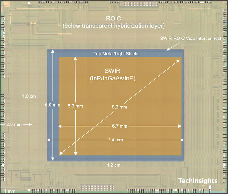
Figure 1: Sony IMX990 Optical Die Photo

Figure 2 (a): Sony IMX990 Optical Image
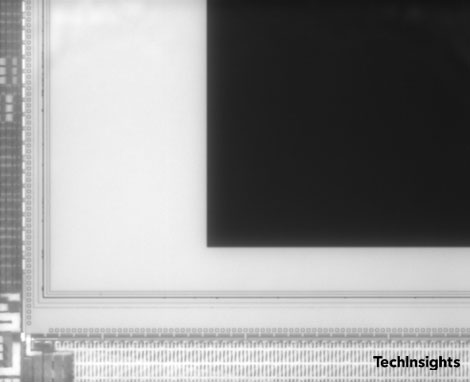
Figure 2 (b): IR Image (~1.7 µm Bandpass Filter)
Sony IMX990 Structure
Figure 3 shows a side-by-side view of the IMX990 SEM cross-section (Figure 3 (a)) along with a corresponding schematic cross-section taken from Sony’s IEDM 2019 publication (Figure 3 (b)). The SWIR and ROIC part are highlighted in both images. The SEM image is taken at the transition between the shielded and active regions of the SWIR Die. It confirms the use of pixel-level Cu-Cu DBI between the SWIR PDA and the ROIC, as indicated on the schematic diagram. We can also see that the pixel-pitch as defined on the schematic, measures 5.0 µm on the SEM image. The SEM image also highlights the top light shield metal, the absorber stack of InP/InGaAs/InP having a total thickness of about 3.4 µm, as well as the bottom metal contact to the SWIR layers. The top n-type InP layer forms a potential barrier at the upper part of the Photodiode and acts as a “Window layer” for Visible light/IR transmission. Its thickness is estimated to be around 0.1 µm (not yet verified). According to Sony, this is critical to ensuring a higher Quantum Efficiency (QE) in the visible range, and makes the IMX990/991 photosensitive to wavelengths from about 0.4 µm to 1.7 µm.
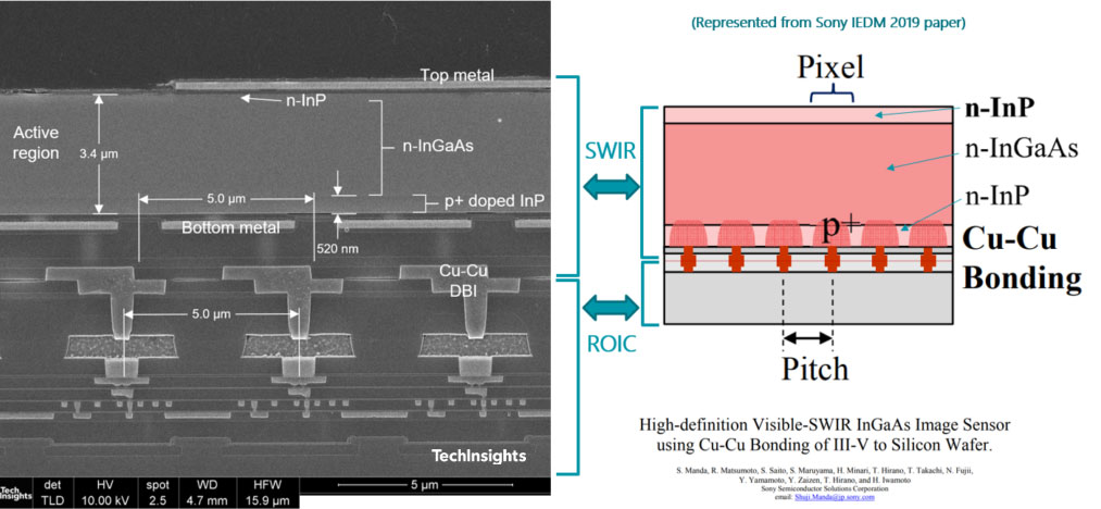
Figure 3 (a): Sony IMX990 SEM Cross Section
Figure 3 (b): Sony IMX990 Schematic Diagram
The main absorber layer is reported to be an n-type InGaAs layer which forms the body of the Photodiode where photon-to-charge conversion takes place. With an applied electric field, it acts as the "Drift" region for charge collection at the bottom. The composition of the absorber layer (while not verified) is expected to consist of In(0.53)Ga(0.47). As, also known as “Standard” InGaAs, as it has a lattice constant of 5.87 Å , a perfect match to that of InP. With a Standard InGaAs absorber, the Energy Gap is around 0.73 eV corresponding to about 1.7 µm cut-off wavelength. The bottom InP layer is 0.582 µm thick and is doped P+ where the bottom metal contact is made. Accordingly, the bottom metal would be biased negatively relative to the top side. Finally, the bottom contact metal connects thru a metal filled via to the SWIR Cu-DBI.
What are competitors doing in this space?
New Imaging Technologies (NIT) announced in February 2021 their NH SWIR technology consisting of a non-bump-bond process for the attachment of InGaAs to ROIC. This of course is to facilitate a smaller pixel pitch SWIR Imager. NIT’s imagers are reportedly only sensitive in the SWIR range of 0.9 µm to 1.7. At present, NIT offers a 1.3 MP InGaAs SWIR imager with a 10 µm pixel-pitch (SenS 1280) as well as a 2048-pixel line scan, with a 7.5 µm pixel-pitch (LiSa SWIR). NIT is reportedly considering smaller pixel-pitch sensors of under 5.0 µm for the future. NIT imagers are on TechInsights’ Image Sensors roadmap, so please stay tuned for upcoming analyses.
Tags: Sony IMX Image Sensor
Ziad Shukri, Subject Matter Expect
Ziad Shukri has more than 25 years experience in R&D and manufacturing of semiconductors and thin-films. In 1996 he joined Analogic Corporation to develop and scale up semiconductor manufacturing technology for amorphous selenium direct converters for Flat Panel x-ray imagers, which lead to a successful commercialization of the technology. After that, in 2007, he joined Redlen Technologies where he worked on single crystal CdZnTe detectors development and manufacturing. Thereafter, Ziad joined TeledyneDalsa in 2010, where he worked on custom CCD process development and CCD/CMOS integration into foundry manufacturing in collaboration with Teledyne Digital Imaging. During his work at Teledyne, Ziad also lead several MEMS projects on pressure sensors and accelerometers for major customers in the automotive sector. He Joined TechInsights as a Senior Technology Analyst in January 2020.
Ziad holds a masters in engineering degree in Photovoltaics and a PhD degree on Ternary semiconductor compounds both from McGill University in Montreal. He is the co-author of several technical publications and two patents.
Find content like this and more in the TechInsights Platform. Sign-up for free today.