Fractilia Dares Chipmakers to Take the Fractilia Challenge

Fractilia Dares Chipmakers to Take the Fractilia Challenge for Up to 20X Better Scanning Electron Microscope Matching and Higher Throughput at No Obligation
“Fractilia Challenge” program invites chipmakers to send SEM images to Fractilia for analysis with its FAME stochastics control product at no cost with unsurpassed tool-to-tool matching results
Austin, Texas, December 6, 2022— Fractilia, the leader in stochastics metrology and control solutions for advanced semiconductor manufacturing, today announced that it has launched a new program that offers chipmakers the opportunity to achieve a 5-20x improvement in SEM tool-to-tool matching and up to 30 percent increased SEM tool throughput using the company’s Fractilia Automated Measurement Environment (FAME™) product at no obligation.
Called the “Fractilia Challenge,” this new program invites interested device makers to perform a small number of experiments with their SEM tools using industry best known methods (BKMs). Fractilia will then measure the SEM images using FAME and prepare a custom report detailing the SEM tool performance as well as potential tool matching and throughput improvements. FAME is the only fab solution that provides highly accurate and precise measurements of CD and a wide range of stochastic effects, which are the single largest source of patterning errors at advanced nodes.
With existing customers, the Fractilia Challenge has enabled a 5-20x improvement in tool-to-tool matching while simultaneously increasing SEM throughput by greater than 30 percent. This matching performance can be achieved not only across SEM tools of the same generation and type, but also between tools of different generations and even different tool vendors. In addition, this breakthrough performance can be achieved for numerous stochastic measurements, including line edge roughness (LER), line width roughness (LWR), local CD uniformity (LCDU) and many others.
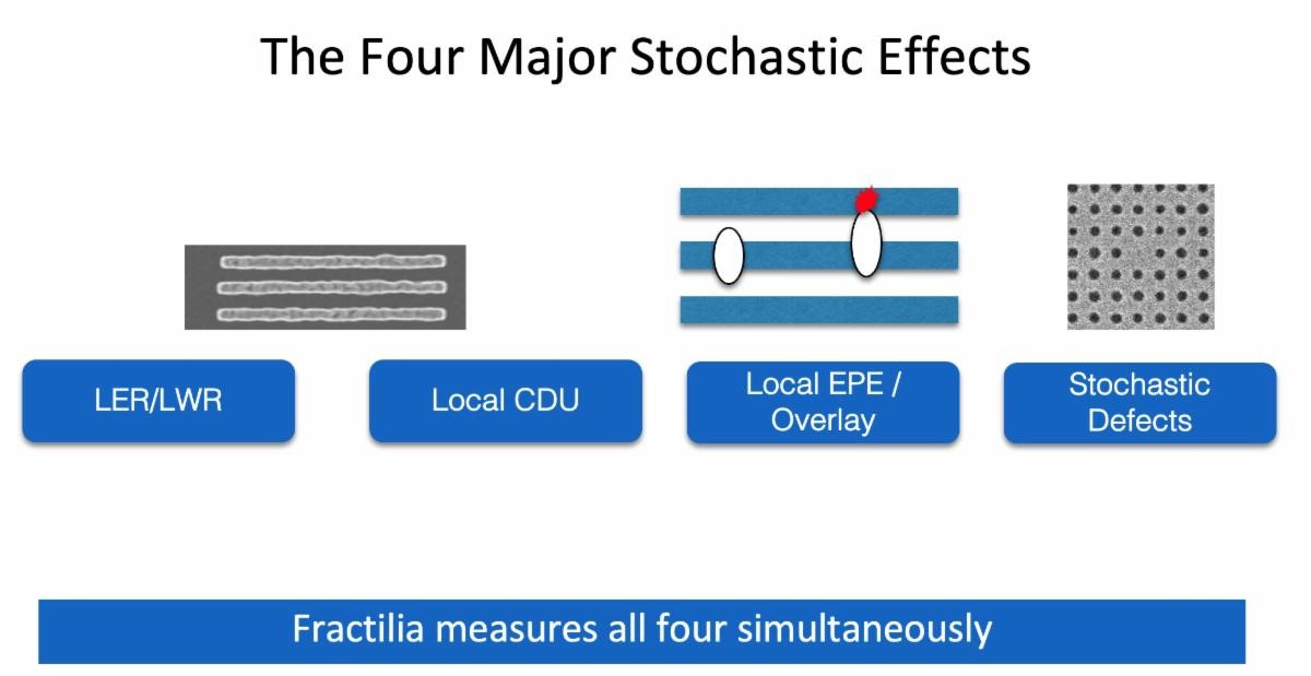
The Fractilia Automated Measurement Environment (FAME™) product from Fractilia measures all major stochastic effects simultaneously, including line-edge roughness (LER) / linewidth roughness (LWR), local CD uniformity (LCDU), local edge placement error (LEPE), stochastic defects, as well as many others.
Benefits of improved SEM tool-to-tool matching through FAME include greater precision and stability in SEM measurements for improved process yield, reduced tool dedication of SEM tools to specific layers for better overall equipment efficiency, as well as the ability to reuse earlier-generation SEM tools for new device nodes, which saves on the cost of purchasing new equipment. By simultaneously increasing SEM throughput without impacting measurement accuracy or precision, FAME also enables customers to use fewer SEMs for the same measurements, further saving money as well as valuable cleanroom space.
According to Ed Charrier, CEO and president of Fractilia, “For the past several decades, chip manufacturers as well as SEM equipment providers have been spending millions of dollars each year to achieve better matching of SEM tools. Fractilia has a unique way to help them achieve better matching with results that they’ve never seen before. For example, with several customers we recently demonstrated the ability to achieve 0.02 nm LWR precision across multiple tools and tool generations. However, we know that seeing is believing, and the Fractilia Challenge is a call to the semiconductor industry to let us prove how well our FAME product enables better matching with chip manufacturers’ existing SEM tool sets, while increasing their throughput, at no obligation to them.”
“Achieving LWR matching between SEM tools of 0.02 nm or less requires an entirely new paradigm for metrology. Many people have told us this level of matching is impossible, but we do it through computational metrology and our ability to measure and subtract out SEM errors to produce a measurement of what is on the wafer rather than what is on the image,” added Chris Mack, CTO of Fractilia.
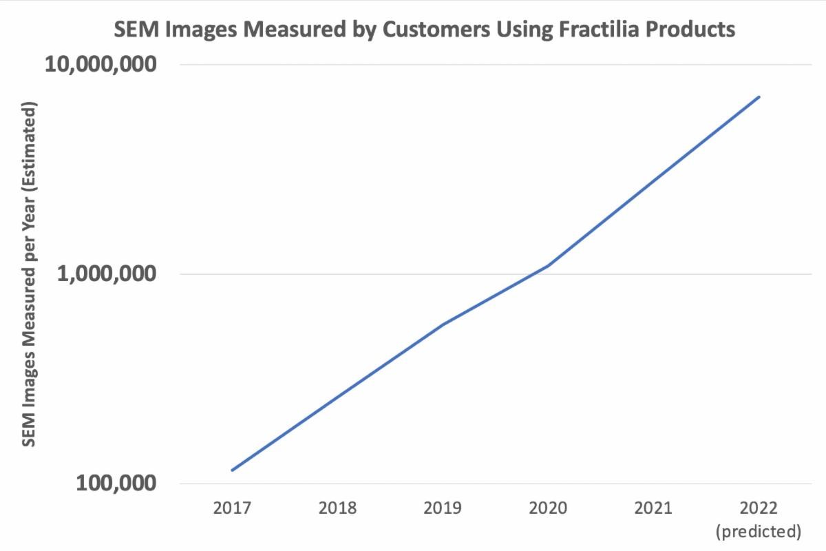
Fractilia has seen an exponential growth with the number of SEM images measured by customers using its products, including FAME.
Fractilia’s FAME product line uniquely provides highly accurate and precise measurement of stochastics, which are random and non-repeating patterning errors that can comprise over 50 percent of the total patterning error budget in EUV processes. FAME uses a proprietary and unique physics-based SEM modeling and data analysis approach that measures and subtracts the random and systematic errors from SEM images to provide measurements of what is on the wafer rather than what is on the images. These “unbiased” measurements of stochastics enable fab engineers to better understand and solve yield issues with their advanced patterning processes, improving their device yields and patterning productivity. The latest release of FAME (FAME 3.1) is built on Fractilia’s proven third-generation Fractilia Inverse Linescan Model (FILM™) platform, which is widely used by the top device makers, research institutes, process equipment providers and semiconductor materials suppliers.
More Information
Fractilia is currently accepting requests to participate in the Fractilia Challenge, but slots are limited. Interested parties should contact Fractilia by email at Takethechallenge@fractilia.com. More information on Fractilia’s FAME solution can be found at https://www.fractilia.com/manufacturing/.
About Fractilia
Fractilia is the leader in stochastics metrology and control solutions for advanced semiconductor manufacturing. Fractilia’s patented Fractilia Inverse Linescan Model (FILM™) technology provides highly accurate and precise measurements of stochastics, which are the single largest source of patterning errors at advanced nodes. As a result, customers can improve device yield and performance, as well as patterning productivity. Fractilia’s offerings are optimizing processes throughout the industry. The company’s solutions include its MetroLER™ product for process development and engineering analysis, and its Fractilia Automated Measurement Environment (FAME™) product for fab ramp and production applications. Fractilia is headquartered in Austin, Texas, and has numerous issued patents and hundreds of trade secrets covering its FILM and related technologies. For more information, visit www.fractilia.com.
Company Contact:
Edward Charrier
CEO and President
Fractilia
Tel: +1.512.887.3646
E-mail: info@fractilia.com
Agency Contact:
David Moreno
Principal
Open Sky Communications
Tel: +1.415.519.3915
E-mail: dmoreno@openskypr.com
Free Newsletter
Get the latest analysis of new developments in semiconductor market and research analysis.
You must be a subscriber to access the Manufacturing Analysis reports & services.
If you are not a subscriber, you should be! Enter your email below to contact us about access.


