Posted: October 31, 2019
Contributing Author: Sinjin Dixon-Warren
Silicon carbide (SiC) is a widely used industrial material. Widescale production by the Carborundum Company started in 1893 following the discovery of the Acheson process, which is still being used. SiC is rarely found in nature, for example in meteorites, as the mineral moissanite. The primary use for SiC has been as an abrasive material, due to its hardness, but it has found uses in automotive brake disks, as an addition to automotive lubricants, and as an alternative to diamonds for jewelry. More recently, it has found use as an electronic material, initially for light emitting diodes (LEDs) and more recently for power electronics devices, including Schottky barrier diodes (SBD’s), junction field effect transistors (JFET’s) and MOSFET transistors. The SiC MOSFET is of particular interest, due to its potential to displace existing silicon super junction (SJ) transistor and integrated gate bipolar transistor (IGBT) technology.
The semiconductor device potential of silicon carbide has been known for many years. In 1962 Lloyde Wallace at Westinghouse patented (US3254280A), a silicon carbide unipolar transistor device. It was essentially a junction FET. Figure 1 shows the Fig. 5 from Lloyde’s 1962 patent. An N-type channel region is formed in a P-type SiC body. Source/drain contacts are formed to the N-type channel. A gate structure is located between the source and drain, with a corresponding gate electrode on the bottom side of the SiC substrate. Silicon carbide based JFET’s are currently in production at UnitedSiC, although to improved performance they are based on vertical design where the source and gate are on the top side of the SiC die and the drain at the back side.
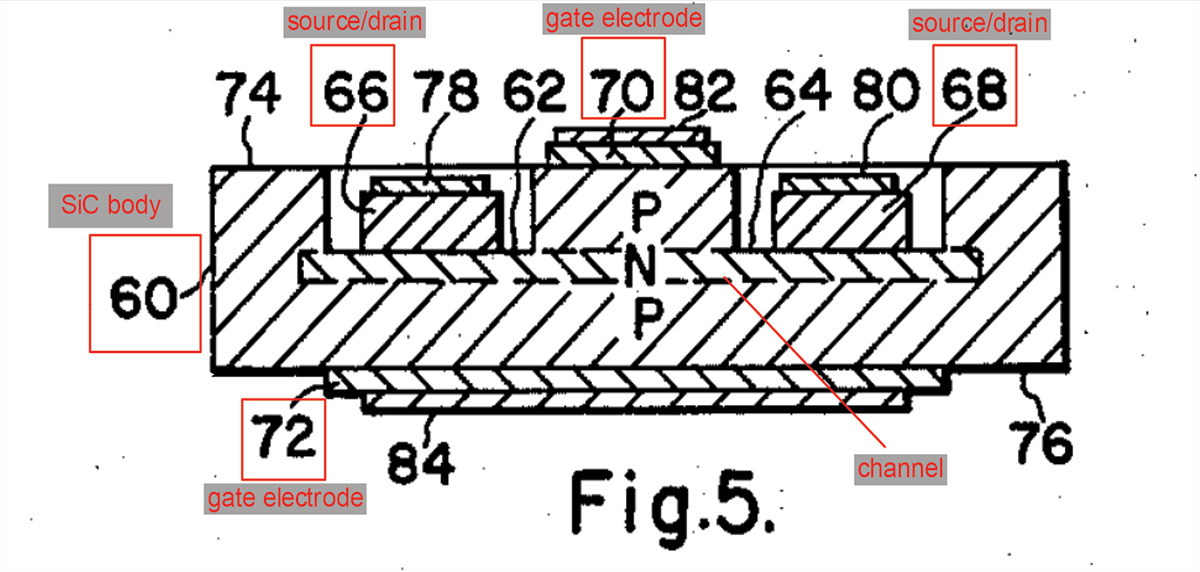
Figure 1 from US3254280A (Silicon carbide unipolar transistor) Fig. 5
The benefits of using SiC for power electronics devices were first described by B. Jayant Baliga of North Carolina State University (NCSU), in 19891. Baliga is best known as the inventor of the IGBT, during his time at General Electric. He is now a Distinguished University Professor at NCSU. He derived a figure-of-merit, denoted BHFFOM, that suggested that power losses could be reduced by using a semiconductor with a larger mobility and higher critical breakdown field, such as SiC or even diamond. Around this time there was a flurry of patent activity relating to power semiconductor applications of SiC.
One of the key inventors at that time was John Palmour, who co-founded Cree in 1987, in the Research Triangle Park, NC; and where he is now the CTO for Power and RF technology. Cree has been one of the major drivers for SiC power device technology. While he was still at NCSU, as a graduate student, Palmour filed in 1987 a critical patent leading to the development of SiC-based MOSFET transistors.
This seminal patent (US4875083A) relates to the formation of a MOS capacitor structure on a SiC substrate. The introduction describes the state of SiC development at that time:
“Silicon carbide has been a perennial candidate for use in semiconductor devices. Silicon carbide has long been recognized as having particular characteristics which give it excellent potential for producing semiconductor devices having superior characteristics to devices formed of other commonly used semiconductor materials such as silicon (Si), gallium arsenide (GaAs), and indium phosphide (InP). Silicon carbide has a wide bandgap, a high melting point, a low dielectric constant, a high breakdown field strength, a high thermal conductivity and a high saturated electron drift velocity. These characteristics give devices made from silicon carbide the potential to operate at higher temperatures, in closer proximity to one another, at higher power levels, and a number of other circumstances under which devices made from other semiconductor materials simply could not perform.
In spite of these known characteristics, commercial quality devices formed of silicon carbide have not been forthcoming. Silicon carbide is an extremely difficult material to work with which crystallizes in well over 150 different polytypes. Accordingly, forming the large single crystals of a single polytype or the thin films of particular polytypes of silicon carbide which are required to produce electronic devices on semiconductor materials has remained an elusive goal.
Recently, however, a number of developments have been accomplished in this field which have made the production of commercial quality electronic devices on silicon carbide possible for the first time.”
Figs. 1 and Fig. 2 of this patent show the structure of the described MOS capacitor, as shown in Figure 2 below. The capacitor is comprised of a circular ohmic contact to the doped SiC substrate with a central circular metal contact over a layer of oxide. The capacitance varies as function of applied voltage due to depletion of the carriers in the underlying SiC. MOS capacitors structures are critical to the formation of MOSFET transistors.
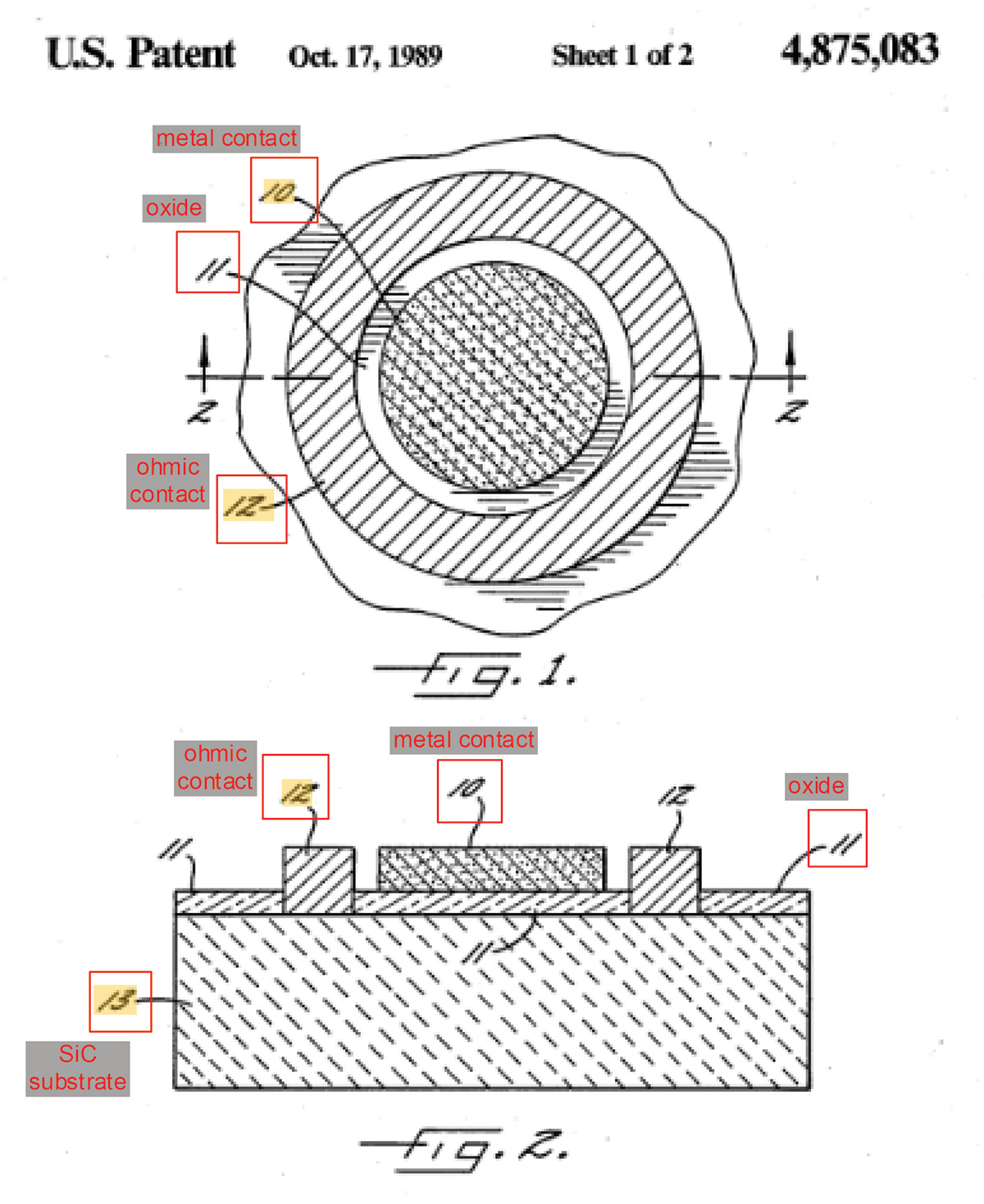
Figure 2 from US4875083A (Metal-insulator-semiconductor capacitor formed on silicon carbide) Figs. 1 and 2
Curiously, an apparatus patent describing a simple planar MOSFET transistor on a SiC substrate does not appear to exist. Likely, the concept would have been considered obvious to “a person having ordinary skill in the art” at that time. There are various patents describing methods for making MOSFET transistors on SiC substrates and there are patents describing variations on the basic structure simple MOSFET structure. For example, Yoshihisa Fujii, Akira Suzuki and Katsuki Furukawa filed US5170231A in 1990 describing a SiC MOSFET with asymmetric source/drain conductivity. Shortly thereafter, in 1992, John Palmour filed his seminal patent (US5506421A) describing the structure of a vertical trench gate SiC MOSFET. The application was granted in 1996, which is now more than twenty years ago, and hence this patent has expired, and the described concept is now in the public domain. There are, however, many SiC MOSFET-related patents that have followed this patent that will still be valid. A search, for example, shows that Cree has more than 700 active patents relating to SiC MOSFET technology.
The described structure of the vertical trench gate SiC MOSFET from Fig. 1 of US5506421A is shown in Figure 3 below. The patent claims a vertical power MOSFET having low on-resistance and high temperature range formed on the C-face of a silicon carbide substrate, likely N-type. An N- drift layer is formed over the substrate followed by a P- channel layer. The trench gate penetrates through the P- channel layer, and N+ source regions are formed. Metal source and drain electrodes are present on the top and bottom sides of the die, respectively. This trench architecture is sometime denoted UMOS (U-shaped gate) to distinguish from planar DMOS (drift MOS) designs.
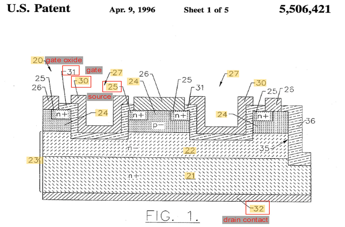
Figure 3 from US5506421A (Power MOSFET in silicon carbide) Fig. 1
We now fast forward to 2011, when Cree launched the first SiC power MOSFET on the market, namely the CMF20120D device. The CMF20120D is a vertical N-channel, enhancement-mode, SiC MOSFET. TechInsights completed a structural analysis of this device shortly after it appeared on the market. Figure 4 shows a cross-sectional SEM micrograph of the planar transistor gates in the CMF20120D device. The N+ source and P-type body implants have been delineated in this SEM micrograph. The CMF20120D is still available from the Wolfspeed division of Cree.
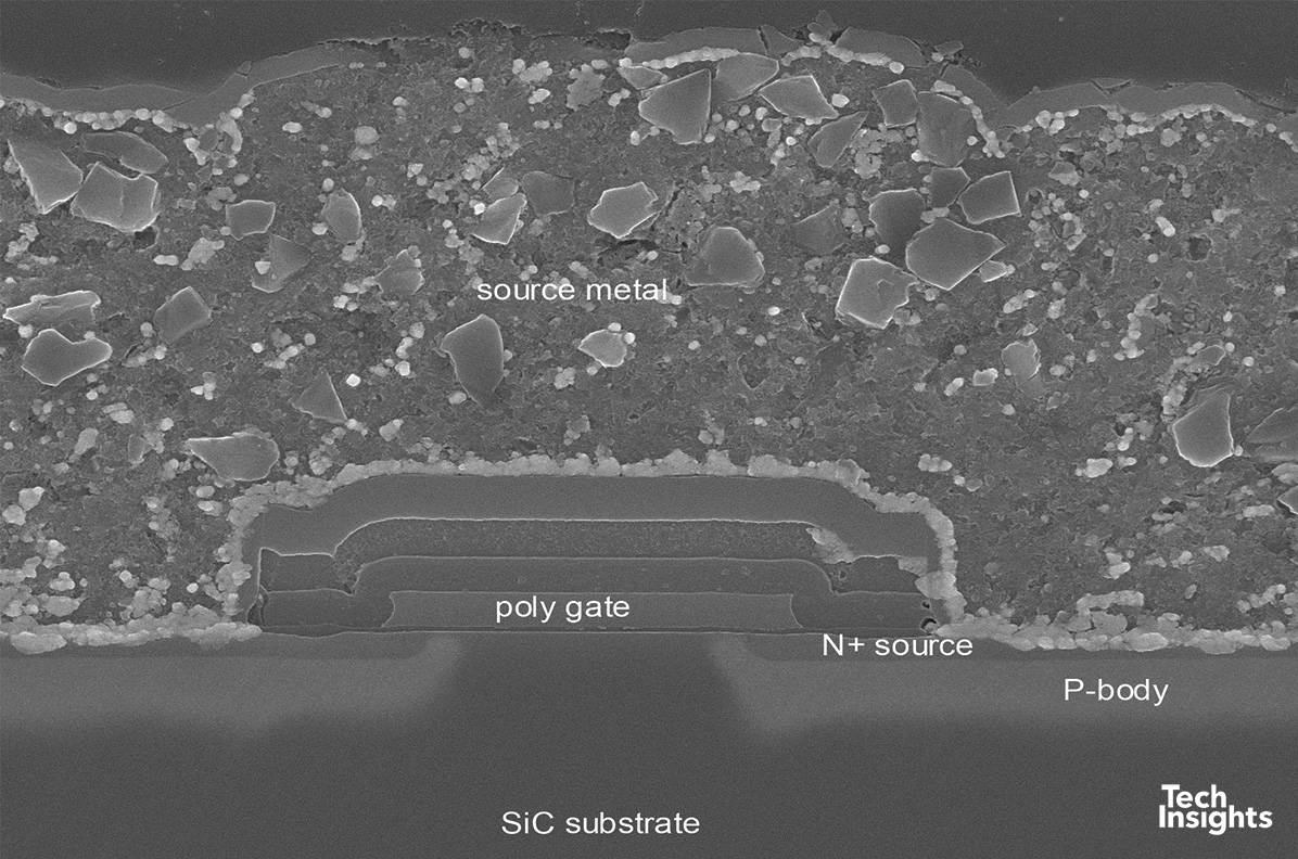
Figure 4 Cree CMF20120D Silicon Carbide Planar MOSFET Cross-Section
Since 2010 the SiC power MOSFET market has expanded markedly and it now exceeds $200 million per year. Many new players have entered the markets, and double-digit compound annual growth is expected, as SiC displaces Si technology in various market, including automotive, photovoltaic, and rail. Typically, SiC power MOSFET have been engineered to operate at 1200 or 1700 V, where they aim to displace IGBT technology. More recently 650 V SiC MOSFET devices have been announced, which likely aim to compete with Si super junction and with GaN-based technology.
It appears that Cree has continued to focus on planar SiC MOSFET technology (ref); however, other players including Infineon and Rohm offer the trench or UMOS technology. STMicroelectronics, by contrast, has also focused on planar SiC MOSFET technology. Figure 5 shows a cross-sectional SEM micrograph of the trench gates found on the Rohm SCT3022AL 650 V SiC N-channel MOSFET. TechInsights has subjected this device to a complete structural analysis2.
Comparison of Figure 5 with Claim 1 ofUS5506421A shows that the Rohm SCT3022AL uses many of the features claimed in John Palmour seminal trench SiC MOSFET patent. For example, the SEM image shows the presence of a trench, an insulating layer, and a gate electrode. Further detailed analysis, including transmission electron microscopy (TEM) and scanning microwave impedance microscopy (sMIM), would be required to demonstrate which claim elements are being used.
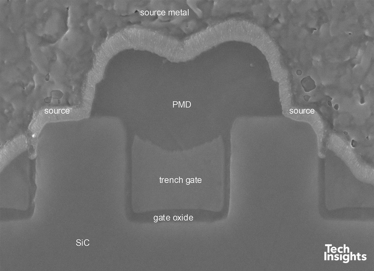
Figure 5 Rohm SCT3022AL 650 V SiC MOSFET Cross-Section
Silicon carbide is a disruptive technology that is beginning to get market traction as it displaces silicon-based technologies in various key power electronics market. Innovative work done by key inventors since the mid-1980’s has made this possible. Projections are that the SiC power electronics market will exceed $1B by 2025, and possibly sooner (ref).
1 B. J. Baliga, “Power semiconductor device figure of merit for high frequency applications.” IEEE Electron Device Letters 10 (10), 1989.
2 Rohm Semiconductor SCT3022ALGC11 SiC MOSFET Power Essentials, PEF-1905-802, TechInsights Inc. 2019.

Get regular, succinct analysis of emerging power process semiconductor products
Fact-based analysis of emerging power semiconductor technologies using Gallium Nitride (GaN) and Silicon Carbide (Sic), and innovative, competing use of Silicon (Si).