The EPC 2152 – A Fully Integrated GaN Half-Bridge IC
We are observing an increasing trend of integrating analogue circuitry onto gallium nitride GaN power high electron mobility transistor (HEMT) die. Navitas has pioneered this approach at higher voltages (>100 V) with its ‘GaNFast’ technology. Multiple competitors have taken an alternative integrated power stage (IPS) approach.

Stephen Russell (Co-authored by Eugene Hsu)
EPC 2152 - Fully Integrated GaN Half-Bridge IC
Wherein the GaN HEMT die is co-packaged with a Si based driver IC. Power Integrations, ST Microelectronics, Infineon and Texas Instruments have all taken this approach, recently we even saw Navitas’ 3rd generation ‘GaNFast’ with ‘GaNSense’ incorporating a Si based IC in our GaN power floorplan report of the NV6134 found within a Xiaomi 120 W USB-C charger.
The main two reasons for integration in GaN are:
- Reducing parasitic inductance from bond wires to maximise the switching performance of GaN devices (one of GaN as a power device material’s most appealing properties)
- Reducing component count and hence product footprint and packaging complexity.
In an integrated power stage arrangement, a half-bridge circuit would require at least three separate die (high-side and low-side GaN power HEMT plus Si IC driver plus associated wire bond and potentially differing die attach). More depth on this can be found in our recent blog on approaches to GaN packaging.
The EPC2152 product from Efficient Power Conversion (EPC) comes in a chip scale package measuring just 3.8 mm x 2.6 mm x 0.6 mm operating at 80 V and 12.5 A. For comparison The Texas Instruments LMG5200 of IPS design has a package size of 8.0 mm x 6.0 mm x 1.6 mm, it operates with the same voltage (80 V) and marginally lower current (10 A).
A demo board from EPC (EPC9146) demonstrates a 400 W inverter for low-cost BLDC motors measuring just 81 mm x 75 mm achieving greater than 98.4% efficiency using the EPC2152.
These advantages of course need to be balanced against power system flexibility i.e. the ability to change components within the driving circuit as well as the additional complexities in the device qualification process and product yield.
Subscribe to TechInsights Blogs
Join our list to get the latest blog posts directly in your email.
A Combination of Innovative Fabrication Techniques
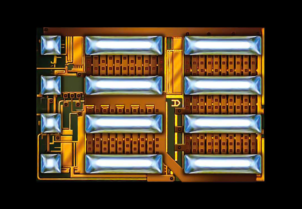
Beyond the small product size, we observe several other innovations throughout the GaN die. None of which alone are necessarily disruptive, but collectively they form an impressive unique product. Figure 1 taken from our recent power essentials summary shows the half bridge GaN IC layout at the gate and source/drain contact levels.
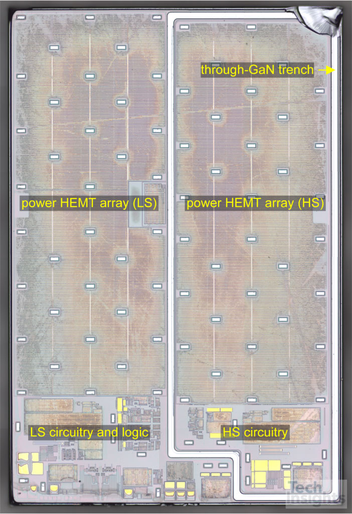
Figure 1. Block annotation of EPC2152 deprocessed die.
Figure 2 shows a general overview of the HEMT arrays. At first glance they are typical compared to similar GaN HEMTs we have observed <= 100 V. Two metal layers are utilised, P-GaN regions are present beneath the gate contact to provide enhancement mode (normally-off) operation and a source connected field plate is employed. The drain-drain pitch is identical for both high and low side HEMTs giving approximately similar specific on-resistance (RDS(ON)*A) for each HEMT.
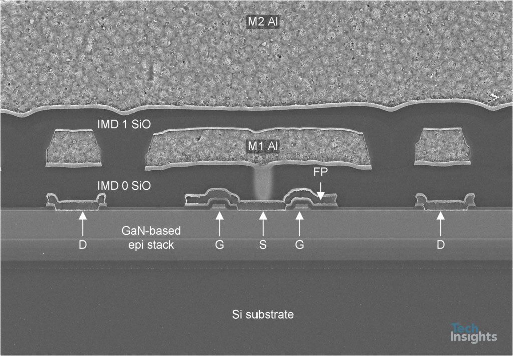
Figure 2. Overview of an EPC2152 GaN HEMT array.
When looking more closely at a plan view of the HEMT arrays we can see one of the innovative features. Figure 3 shows a staggered GaN etch shallow – deep – through GaN to create a contact to the underlying Si substrate, these are present throughout the die, in both high and low side HEMT arrays as well as driver/logic circuitry. A through-GaN etch is also used in the region around the high-side HEMT to create an isolation trench and at the die edge as a crack-stop. This substrate contact is a relatively new innovation in GaN devices, although we did also observe it in our power essentials report of the Texas Instruments LMG5200.
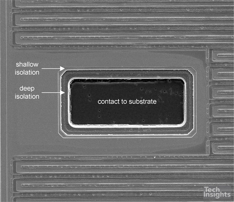
Figure 3. Contact to substrate visible in plan view SEM of GaN HEMT array region.
Ensure you’re armed with the latest technical intelligence.
Sign up for a free trial today to see how the TechInsights Platform will help you.
Sample reports from this blog may be available with your free trial.
Electrical isolation between individual GaN HEMT devices and from HEMTs to analogue circuitry is crucial. The ability to etch through the entirety of the GaN epitaxy suits this purpose well, separating high voltage regions from low.
The purpose of the contact to substrate is particularly interesting. EPC demonstrated a patent for this technology as far back as 2010. Similar methods are also described in academic literature to suppress the backgating effect in a monoloithically integrated half-bridge. In this paper the contact to underlying silicon enables both substrate and source to be kept at the same potential, albeit for a SOI device.
Figure 4 shows a cross-section of the contact, deep GaN epi etch and shallow GaN epi etch.
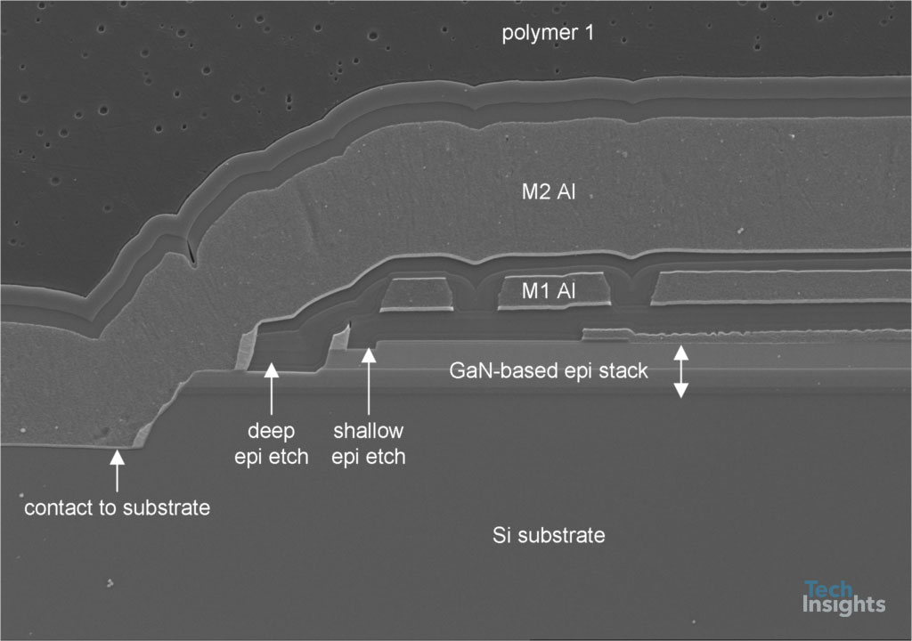
Figure 4. Cross-section view of contact to substrate.
Further Innovation –Driver Circuitry and Gate Stack
In the analogue circuit region we observed smaller HEMT structures, resistors and MIM capacitors all utilisng the same process flow as the HEMT itself. These provide gate drive for the GaN HEMTs along with additional functionality such as detection and protection.
Finally looking at a TEM image of the gate stack as shown in Figure 5 we see as well as the p-type region beneath the gate contact there are additional thin AlGaN and GaN layers present within this stack. These may be related to improving device reliability and suppressing gate leakage current.
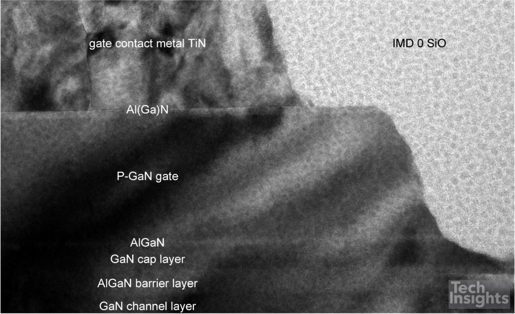
Figure 5. Additional GaN & AlGaN layers observed in the gate stack.
Summary
With both high-side and low-side GaN HEMTs having RDS(ON)*A of ~0.3 mΩ.cm2 they compare favourably to the Texas Instruments LMG5200 IPS. Both high-side and low-side GaN HEMTs in this product have RDS(ON)*A of ~0.5 mΩ.cm2.
When comparing to equivalent discrete 100 V GaN HEMTs in the market the GaN HEMTs on this IC are also competitive, for example we measured the GaN Systems GS61008P to be ~0.8 mΩ.cm2 while EPC’s EPC2218 device was ~0.2 mΩ.cm2. This impressive on-state performance coupled with the enhanced switching that integration will provide makes this product appealing for those looking for a ready-made device for its specified applications (converters, motor drivers and class D audio amplification).
Another GaN IC we recently analysed from EPC is the EPC21601 ToF laser driver IC featured in a GaN power floorplan report. This also shows the diversity of applications GaN can appeal to and reaffirms in power semiconductor devices there is not a ‘one size fits all’ approach. These kind of low voltage applications are practically out of reach of silicon carbide (SiC), conversely at much higher voltages there are applications where the opposite is true.