DRAM Scaling Trend and Beyond

Dr. Jeongdong Choe
When it comes to DRAM cell scaling, we refer to the cell pitch trends from Samsung, SK Hynix, and Micron DRAM products, including active, WL, and BL pitches.
Although Micron has been changed cell design and removed the isolation gate line since D1x generation, all the pitches have been scaled-down generation by generation. Active pitches are smaller than WL and BL pitches, and a 6F2 cell design has been a mainstream to date.
Once we keep 6F2 cell design and process integration, including BCAT cell structure, bulky saddle fin-type active, storage node landing pad and plug, BL air-gap spacer, cylindrical or quasi-cylindrical capacitor, and COB (capacitor-on-BL) with AlO/ZrO based capacitor dielectrics, DRAM technology extension may have the limitation. Here, from DRAM D/R trend from major players on current and near-future generations such as 1z, 1b, and 1c benchmarking results, it’s getting saturated and 10 nm may will be the last node for 6F2 DRAM cell.
DRAM foundries are eager to extend this by developing more innovative technologies, materials, and methodologies such as gate work-function engineering, HKMG, sensing margin, and speed improvement, row-hammer scaling, and higher-NA EUV tools (Figure 1). After that, a few different approaches and prototypes will be needed for higher density, higher performance, and higher speed for DRAM cell integration around 2028 or later, for example, 2T0C capacitorless DRAM cell with indium-gallium-zinc-oxide (IGZO) thin-film transistors (TFTs).

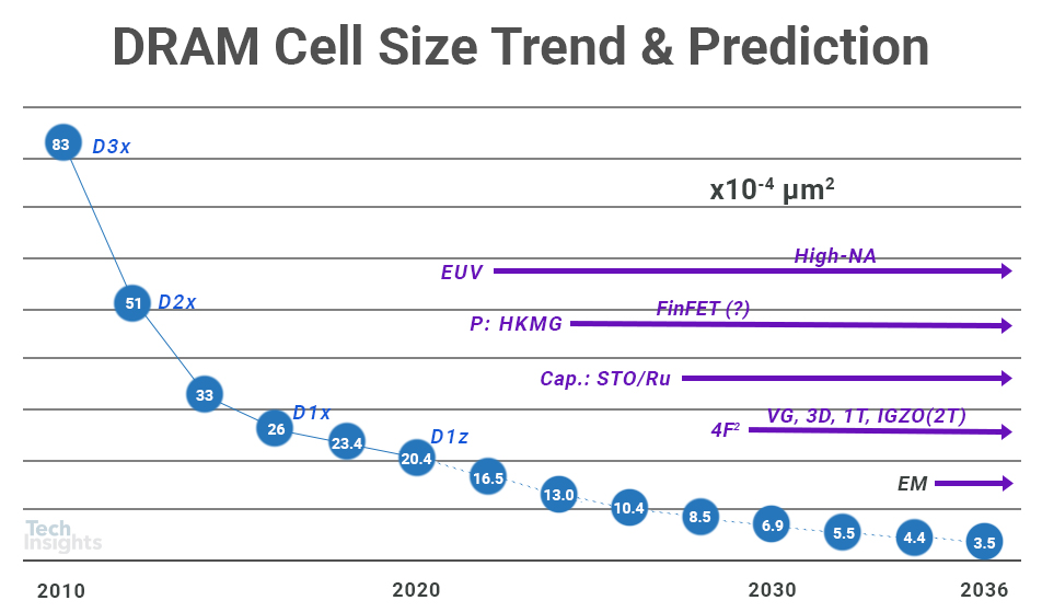
Figure 1. DRAM Cell Size Trend and Technology Prediction
Regarding the DRAM cell scaling and operation, cell capacitance is one of the keywords. DRAM cell capacitance has been decreased on and on as device scales, and D1z and D1a cell capacitances are now lower than 10 fF/cell. The high-k dielectric layer thickness was shrunk as well down to 7 or 6 nm to increase the capacitance. Capacitor process integration already changed from cylindrical capacitor to quasi-cylindrical capacitor, for example, from SK Hynix D1y and D1z generation and Samsung D1z generation, and high-k dielectric materials changed and optimized, for example, from Micron D1y and D1z generation.
Due to these changes, SK Hynix, for example, adopted a new S/A transistor structure such as a recessed channel to improve TR reliability. From the physical limitation on cell design, cell capacitance may will be further decreased more down to 6 or 5 fF/cell for D1c generation, however, manufacturers would like to keep it up with more than 6 or 7 fF/cell. To do this, more reliable and ultra-thin higher-k dielectric layer deposition tools should be developed and applied.
The reduction of the leakage current with a ZrO2(NbO)/Al2O3-based nanolaminate for a sub-10 nm technology node is likely unrealistic. We know that further scaling down the cell and capacitor while maintaining the cell capacitance (> 7fF/cell) becomes very difficult and will require materials with a higher dielectric constant (k > 50). One of the candidates for capacitor materials will be strontium titanate (STO) with Ru electrodes with typically a bandgap below 3.5 eV. In this case, Ru will be a metal of choice due to its high work function positively affecting the leakage current density by ensuring a high conduction band offset between electrode and dielectric. In addition, Ru oxide is conductive and hence will not contribute to the EOT. Scalability of STO/Ru looks possibly < 0.5 nm EOT.
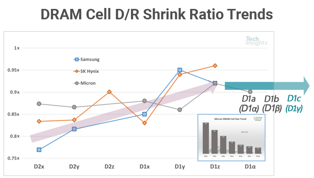
Figure 2. DRAM Cell D/R Shrink Factor (SF) Trend
DRAM cell integration has been kept a 6F2-based cell design for every DRAM foundry. Regarding the D/R (design rule) on DRAM cell, Figure 2 shows a trend of shrink factor (SF) on DRAM D/R for Samsung, SK Hynix, and Micron, D2x through D1z generation. For example, Micron had been kept 0.75 ~ 0.85 for many years, however for their D1z, the shrink factor increased to 0.92. For Samsung and SK Hynix, SFs also increased generation by generation.
Especially for D1z generation, they’re more than 0.92, which means it’s getting harder to shrink DRAM cells. SF on DRAM cell may will keep over 0.9 for a while on the next three generations, D1a, D1b, and D1c, for 6F2 BCAT 1T+1C integration.
eBook: 2022 and Beyond for Memory Technology
Insights, Analysis and Trends by Dr. Jeongdong Choe
(Senior Technical Fellow, TechInsights)


