Technology Blog
Comparison: Latest 3D NAND Products from YMTC, Samsung, SK hynix and Micron
Chi Lim Tan
January 11, 2023
With their 232-layer Xtacking 3.0 readily available in commercial products, YMTC appears to have pulled ahead of the pack for the moment. TechInsights ran a comparison of the YMTC 232-L against 128- and 176- layer solutions from Samsung, SK hynix, and Micron, looking at factors like die size, bit density, active layers, word line pitch, and more.
Share This Post
As TechInsights continues analysis of YMTC 232-Layer 3D NAND, we thought a comparison was in order. We compared the YMTC’s 1024 Gb (1 Tb) triple level cell (TLC) 232-L 3D NAND with recent 512 Gb TLC 3D NAND dies (see Table 1) we examined from Samsung, SK hynix and Micron.
| Metrics | YMTC 128-L | YMTC 232-L | Samsung 128-L | Samsung 176-L | SK hynix 128-L | SK hynix 176-L | Micron 128-L | Micron 176-L |
| Die markings | CDT1B | EET1A | K9AHGD8U0B | K9AHGD8U0D | H25FTB0 | H25FTC0 | B37R | B47R |
| Die size (seal) area (mm2) | 60.42 | 68.15 | 73.60 | 47.10 | 63.00 | 46.50 | 66.08 | 49.84 |
| Memory capacity (Gb) | 512 | 1024 | 512 | 512 | 512 | 512 | 512 | 512 |
| Bit density (Gb/mm2) | 8.47 | 15.03 | 6.96 | 10.87 | 8.13 | 11.01 | 7.75 | 10.27 |
| Number of active layers | 128 | 232 | 128 | 176 | 128 | 176 | 128 | 176 |
| Number of decks | 2 | 2 | 1 | 2 | 2 | 2 | 2 | 2 |
| WL pitch (nm) | 58 | 48 | 44 | 43 | 52 | 45 | 56 | 56 |
| BL pitch (nm) | 39 | 39 | 38 | 38 | 38 | 38 | 38 | 38 |
| VC height (μm) | 8.5 | 12.4 | 6.6 | 8.9 | 8.1 | 9.4 | 8.6 | 10.7 |
| Slit depth (μm) | 8.8 | 12.7 | 6.7 | 9.2 | 8 | 9.3 | 9 | 11 |
Table 1: Comparison of recent 3D NAND. TechInsights, 2022.
Up to and including 128-L, 3D NAND had been dominated by Samsung with its single deck process, enabled by its ultra-high aspect ratio (UHAR) hole etch. Samsung still leads the pack with the smallest word line (WL) pitch, which allows more layers to be stacked while minimizing the impact to the process requirements for vertical channel (VC) height and slit depth. While it appears that Samsung may have had the lowest process cost for 128-L, it did not have the lowest die size. This is significant, because the lower the die size area, the more dies that can be fabricated on a 300 mm wafer, and thus more profit.
Samsung started to adopt the cell over periphery (COP) approach at 176-L (Samsung’s 7th-generation 3D NAND) which lead to a significant die size reduction from its 128-L to 176-L. Similar approaches had been used by Micron from 32-L (Micron’s 1st-generation 3D NAND) onwards, which Micron termed as CMOS under array, CuA, and by SK hynix from 96-L (SK hynix’s 4th-generation 3D NAND) onwards, which SK hynix termed as 4D NAND, periphery under cell or PUC). YMTC applied Xtacking at 64-L (YMTC’s 2nd-generation 3D NAND) to achieve similar benefit of reduced die size, by having the memory array over the periphery circuits. The reduced die size along with increased active word lines (AWLs) drives up the bit density.
The recently acquired YMTC 232-L six-plane 1 Tb TLC die with center X-decoder (see Figure 1) has the highest bit density of 15.03 Gb/mm2.
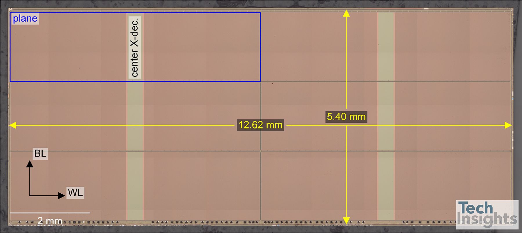
Figure 1: Die image of YMTC 232-L 1 Tb die. TechInsights, 2022.
Chart 1 shows bit density (Gb/mm2) versus number of AWLs. We expect the bit density of the upcoming 232/238L dies to reach approximately 15 Gb/mm2. At ISSCC 2022, Samsung 2xx-L test vehicle (with four-plane 1 Tb TLC die with edge X-decoder) has a bit density of 11.55 Gb/mm2 [1]. We expect the bit density to increase to above 14.5 Gb/mm2 when the production mask set is used. SK hynix 238-L six-plane 1 Tb TLC die with center X-decoder is estimated to be 14.75 Gb/mm2 [2] with 34 % increased from previous generation. Micron 232-L six-plane 1 Tb TLC die is stated to be 14.60 Gb/mm2 [3].
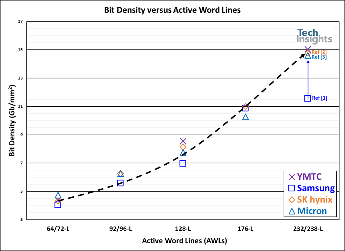
Chart 1: Bit Density versus Active Word Lines (AWLs). TechInsights, 2022.
Several TechInsights Memory Floorplan and Advanced Memory Essentials reports informed this comparison article. Subscribers to our NAND & DRAM channels can access the reports below in our Platform. If you are not a subscriber, but are interested in our reports, please contact us.
| Key Players | 64/72-Layer | 92/96-Layer | 128-Layer | 176-Layer | 232/238-Layer |
|---|---|---|---|---|---|
| YMTC | MFR-2003-801 | - | MFR-2211-801 | - | MFR-2211-804 |
| Samsung | MFR-1903-802 | MFR-1903-803 | MFR-2102-804 | MFR-2211-803 | Reference [1] |
| SK hynix | MFR-1811-801 | MFR-1909-801 | MFR-2008-805 | MFR-2206-801 | Reference [2] |
| Micron | MFR-1902-806 | MFR-1902-807 | MFR-2104-802 | MFR-2107-805 | Reference [3] |
Table 2: Information sources for Chart 1. TechInsights, 2022.
At 232/238-L, YMTC showed the highest bit density and Samsung is projected to have the lowest bit density. What does this mean for the NAND market? Does this mean that Samsung will be dropping out of the race? Certainly not. One of the more important factors to consider is the overall cost, and thus the metric of cost/bit is the most ideal data for comparison. TechInsights, through our recent acquisition of IC Knowledge, is working toward calculating cost/bit, and should have this information available in 2023. IC Knowledge is the world leader in cost modeling of semiconductors. Click here if you would like to learn more about this acquisition.
Reference:
[1] M. Kim et al., "A 1Tb 3b/Cell 8th-Generation 3D-NAND Flash Memory with 164MB/s Write Throughput and a 2.4Gb/s Interface," 2022 IEEE International Solid- State Circuits Conference (ISSCC), 2022, pp. 136-137, doi: 10.1109/ISSCC42614.2022.9731640.
[2] SK hynix Press Release: https://news.skhynix.com/sk-hynix-develops-worlds-highest-238-layer-4d-nand-flash
[3] Micron Product Information: https://www.micron.com/products/nand-flash/232-layer-nand
[4] TechInsights Press Release: https://www.techinsights.com/press-release/techinsights-acquires-ic-knowledge-llc
More of our coverage on YMTC’s Xtacking 3.0 https://www.techinsights.com/disruptive-event/ymtc-232l-tlc-3d-nand


