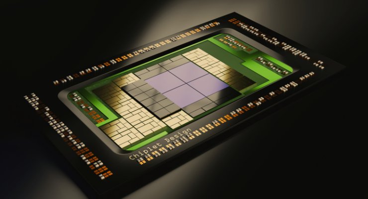
Chiplets, a new design methodology?
The Chip Insider®
Author: G. Dan Hutcheson
The article from TechInsights discusses the emergence of chiplets as a transformative design methodology in the semiconductor industry. Chiplets involve integrating multiple dies onto a single substrate, enabling the creation of complex System-in-Package (SiP) architectures.
The article highlights the historical context of chiplet technology, dating back to Jack Kilby's Integrated Circuit in 1958, and explores recent developments such as the Universal Chiplet Interconnect express (UCIe) initiative. It also discusses the advantages of chiplets, including improved yield optimization, performance scalability, and opportunities for innovation in areas like testing and design automation. Overall, the article emphasizes the significant impact chiplets are poised to have on semiconductor design and manufacturing processes.
Free Full Access to The Chip Insider®
Unlock exclusive insights into The Chip Insider® by logging into the TechInsights Platform today!
Access in-depth analyses and stay ahead of industry trends.


