Image Sensors Technology
Automotive Image Sensor Highlights

Ziad Shukri
TechInsights recently attended AutoSens Brussels 2022, held September 12-15th at Autoworld in central Brussels.
A word about Autoworld, the museum is probably the most appropriate site for a conference focused on the future of automotive transport. It houses a vast collection of vintage cars from the early 1900s to the 1960s and 70s (collected by the Mahy family). Seen side-by-side with emerging Advanced Driver Assistance Systems (ADAS)-equipped vehicles on display, it highlights a contrasting reminder of the technological journey the Automotive sector has undergone (and still is going through).
AutoSens Brussels 2022 hosted key industry stakeholders, including CMOS Image Sensor (CIS) providers Onsemi, Sony, OmniVision and Samsung, Image Signal Processing (ISP) providers arm, nextchip, and AI-chip vendor GEO Semiconductor. LiDAR/3Dsensing companies attending included Baraja, Samsung Institute of Advanced Technology (SAIT), Cepton, TriEye, Algolux and IMEC.
This blog provides some highlights of recent CMOS Image Sensors developments and trends from AutoSens Brussels.

Figure 1. Autoworld, AutoSens Brussels 2022.
Onsemi
Onsemi presented work on their latest High Dynamic Range (HDR) image sensor incorporating LED Flicker Mitigation (LFM) for ADAS/AV applications. The new automotive sensor (reported to be the AR0823) has a resolution of 8.3 MP and a 2.1 µm pixel-pitch.
According to Onsemi, a resolution of the order of 8 MP is required for ADAS automotive applications to resolve small objects such as a brick or a rock up close or larger objects as cyclists or pedestrians at much greater distances of 100s of meters. In terms of High Dynamic Range (HDR), the AR0823 uses Onsemi’s super-exposure (SE) pixel technology, with a very large Full Well Capacity (FWC) photodiode plus an in-pixel Over-Flow Capacitor (OFC) to deliver one of the industry’s highest reported overall dynamic range of 150 dB.
Such a dynamic range is achieved in two successive (Staggered) exposures, a first “long” exposure that captures a lower illumination range delivering ~ 110 dB, while the 2nd “shorter” exposure captures higher illumination and provides the remaining ~ 40 dB HDR. Onsemi reports minimal image blurring across the dynamic range and a full LFM capability. The LED Flicker is primarily captured through the 1st exposure where, full LFM capability is achieved.
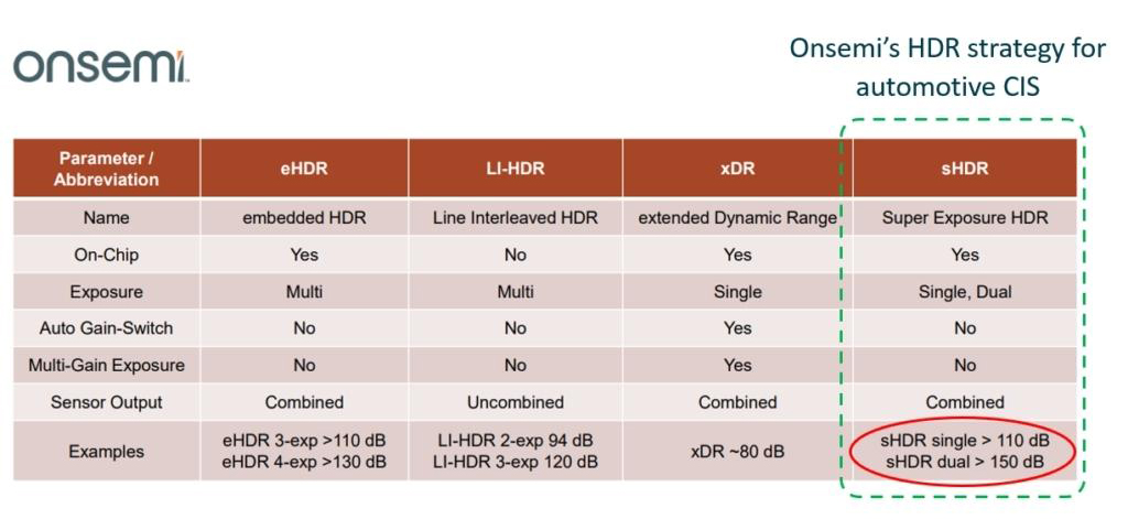
Figure 2. Comparison of different High Dynamic Range (HDR) strategies (source: Onsemi presentation at Image Sensors Europe 2022).
Onsemi compared performance of this 2.1 µm pixel-pitch high FWC + OFC sensor with competing 2.1 µm and 3.0 µm split-photodiode pixel designs. In certain scenarios of light and temperature conditions, Onsemi reports the single super-exposure technology to be superior in terms of overall Signal-to-Noise Ratio (SNR) and Modulation Transfer Function (MTF), thereby allowing better object detection at corner cases.
Onsemi is also working on a lower resolution, 3.0 MP sensor with the same HDR range of 150 dB that is expected to be announced soon. Both the AR0823 and the newer sensor have Rolling Shutter, which according to Onsemi, provides up to ~ 60 fps output, sufficient for current automotive scenarios while avoiding Global Shutter pixel complexity and cost.
According to Onsemi, the automotive camera requirements are defined by the range of objects to detect and the detection criteria. For object recognition, 8 pixels are needed in a high contrast image across the object, while 16 pixels are needed for object identification. Given that ADAS cameras need to detect objects as small as a rock or brick on the road, a resolution of around 8 MP is needed for ADAS applications. This however this depends on the Field Of View (FOV) of the Camera in use. Lower FOV can accommodate lower resolution CIS, but a higher FOV cameras of ~ 140 degrees and more, may require even larger resolutions.
Since most OEMs prefer a small sensor package size with optical formats of ~ 1/3” to 1/2” , pixel pitch has to be chosen to meet such criteria without losing sensitivity at lower illumination. In addition to ADAS uses cases, Onsemi is also adapting its ~ 8 MP resolution sensors toward In-Cabin use cases for Driver Monitoring and Occupant Monitoring Systems (DOMS).
Sony
Sony presented work on their “Fuji” pixel architecture for automotive image sensors. Sony also adopts an 8 MP, 2.1 µm pixel pitch CIS which Sony regards as mainstream for Front-sensing automotive CIS. In addition, Sony indicated that such larger resolutions could also address automotive OEMs desire to utilize a single type of camera for a multitude of use cases, helping standardize integration.
Sony’s “Fuji” sensor architecture achieves a high dynamic range using a rather intricate pixel design. It employs both a split Photodiode (PD) approach, a large PD for low illumination and a small PD for higher light levels. The small PD incorporates an in-pixel over-flow capacitor to extend the dynamic range further for high illumination levels. The “Fuji” pixel also incorporates Dual conversion gain on the large Photodiode, a low conversion gain for intermediate illumination, and a high conversion gain, for very low light levels.
Accordingly, this pixel architecture is more involved than the single-exposure large FWC pixel, but Sony believes this compromise design yields the best overall SNR and Dynamic range. The simultaneous exposure of the three pixel-readouts provides a dynamic range of about 108 dB . By incorporating an additional 2nd short exposure of the Large photodiode (low gain), extremely high light illumination such as direct sunlight can be handled. According to Sony, this approach achieves an overall 130 dB of dynamic range under moderate temperature conditions. Figure 3 reproduces the timing sequence presented by Sony.
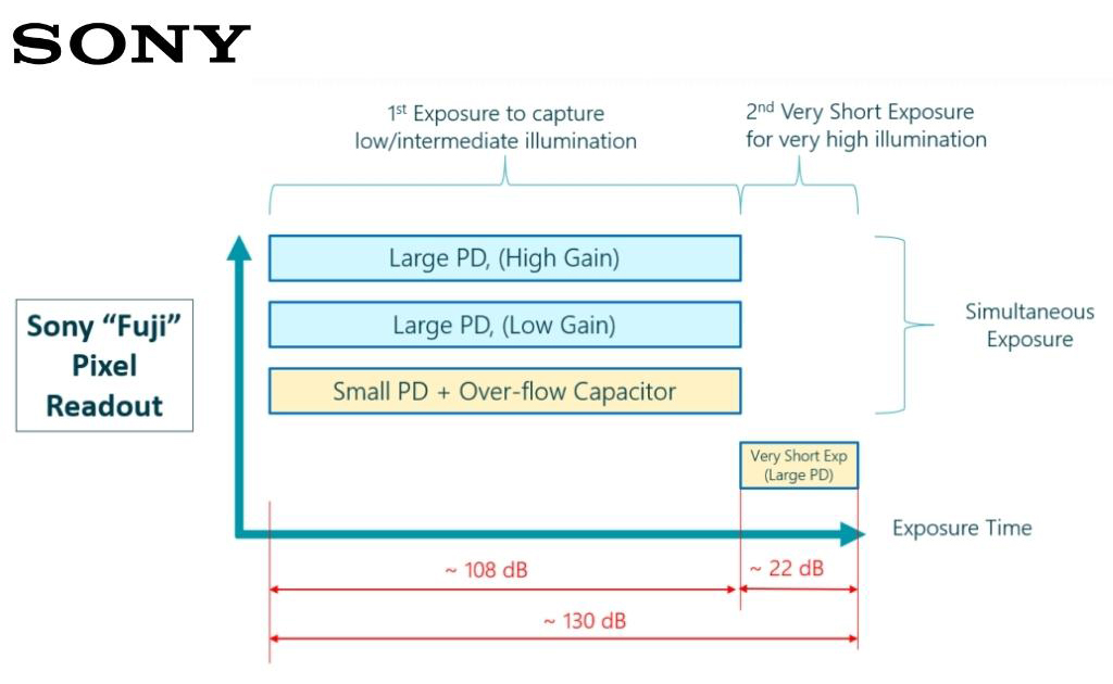
Figure 3. Sony “Fuji” Pixel HDR Readout (Based on Sony AutoSens 2022 presentation).
In terms of output, Sony discussed ways to optimize the image format automotive use where both RAW and YUV output is generated simultaneously for both sensing and viewing. Currently, Image sensor RAW pipeline output is optimized for computer vision (Sensing). Image processing for YUV color perception coding is done downstream and uses RAW input which is not optimal. By integrating a separate and dedicated ISP chip for each of the RAW and YUV image processing, one can process images independently and improve image quality for each use case and standardize camera system architecture for multiple use-cases. If this approach is adopted, it would consist of triple stacked sensors of CIS + ISP1 + ISP2 as the future for Sony’s automotive sensors (Figure 4).
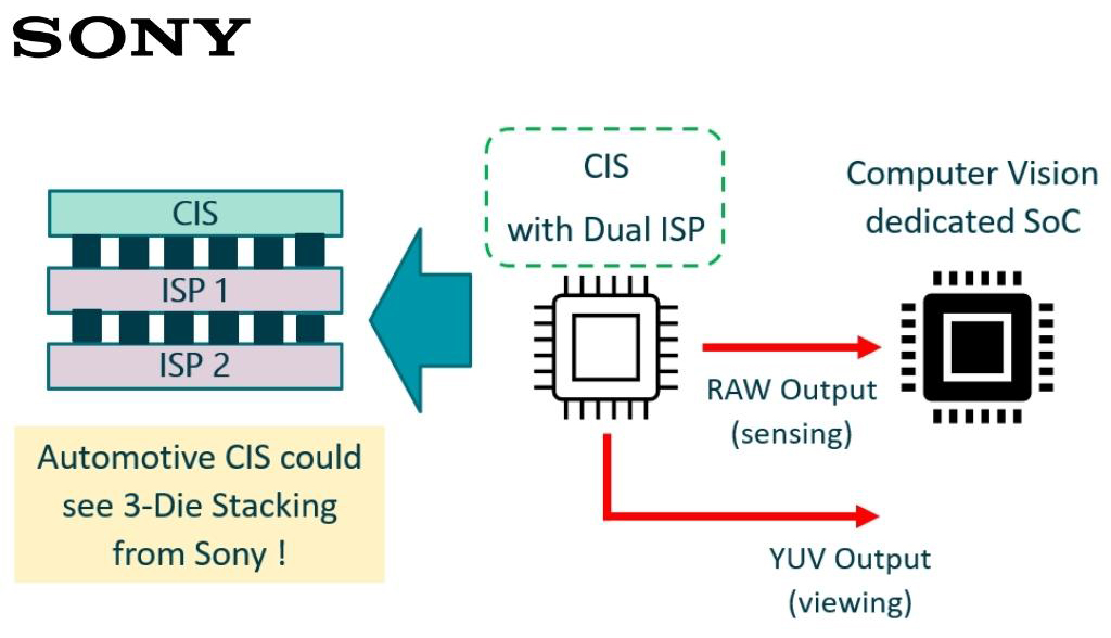
Figure 4. Sony proposed CIS with integrated dual ISP.
OmniVision
OmniVision presented several trends for automotive image sensors in terms of resolution, frame rate and overall data rates. For resolution, OmniVision projects increasing resolution for ADAS / AV cameras, possibly up to 15 MP. The need for higher resolution is two-fold, 1st for optimal detection of objects at greater distances. This affords early detection particularly important at higher speeds, for instance on highways.
The 2nd factor is increasing Field Of View. OEMs are increasing interested in larger FOV cameras to limit the total number of cameras in the future. A larger FOV means greater angular resolution is needed, and therefore a greater CIS resolution. For Surround viewing, OmniVision also foresees a trend of increasing resolution beyond the current 3 MP. That said, current viewing resolution is primarily dictated by the in-cabin display resolution, but larger future displays would require better CIS viewing resolution beyond 3 MP.
In addition to CIS resolution, output frame rates for automotive sensors are expected to increase from the current ~ 30 fps up to 45 or even 60 fps, depending on resolution, but especially needed for Level 4/5 autonomy. These higher CIS resolution and frame rates imply much higher overall data rates for future automotive imaging and that will require greater processing power. More importantly, it will necessitate better quality of data with less uncertainly. In other words, the more on-chip functionality, processing and vetting of information at the camera level, the better and faster the overall system performance (Figure 5).
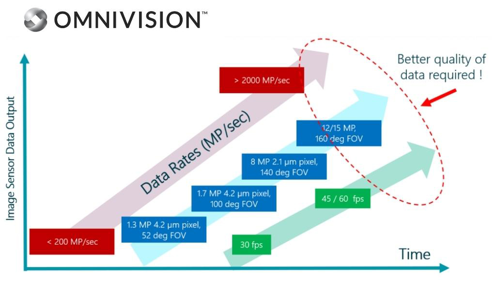
Figure 5. Increasing Data Rates with Increasing Resolution, Frame Rate.
To facilitate such functionality, OmniVision also predicts greater image sensor integration and a transition from 2-Die stacked imagers where current ISP chip house both Analog and Digital circuity to 3-Die stacking where the Analog and Digital logic are segregated into dedicated Die. This allows optimization of process technology for each chip as well as provide reduced Die size, and reduced power (Figure 6).
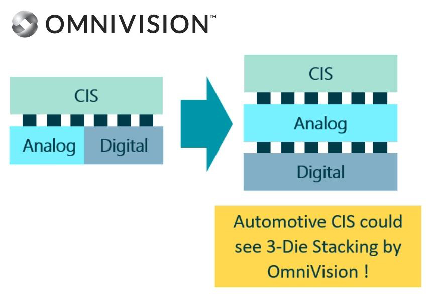
Figure 6. OmniVision predicts 3-Die stacked Automotive sensors with dedicated Analog and Digital ISP Die.
Samsung
amsung did not have a presentation on its automotive image sensors but did have two sensors on display at its booth. The sensors were the 3B6, a 3MP (1920 x 1536) RGB image sensor with a 3 µm pixel-pitch for Surround view, and a higher resolution 8.3 MP (3840 x 2160) RGB sensor the 1H1 with a smaller 2.1 µm pixel-pitch, for Front sensing and viewing applications. Both sensors have Samsung’s split-photodiode “CornerPixel” architecture, and have been deployed for quite some time now.
According to Samsung, Rolling shutter is sufficient for current frame rate requirements for ADAS applications, but In-Cabin/DMS use cases do require Global shutter functionality. It is therefore speculated that both sensor mentioned above are indeed Rolling shutter, as Samsung has not yet reported a dedicated sensor for Driver/Cabin monitoring. It is interesting that the automotive sensor Samsung previously announced, the 4AC, which was also reported to have CornerPixel, has not been observed nor was it on display at AutoSens.
That said, it was reported that Samsung is currently working on a 15 MP resolution automotive sensor, likely to be the 1P1, and is also intended for Front sensing applications, although there is no formal announcement yet.
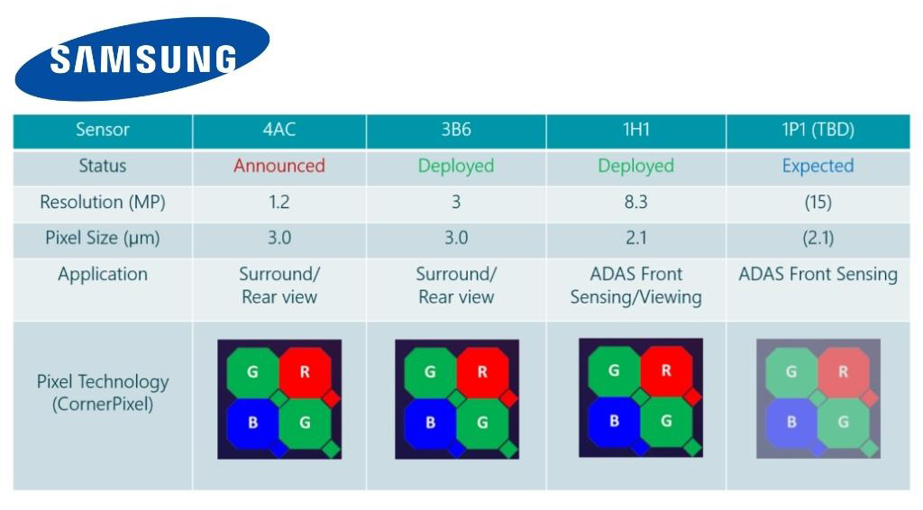
Figure 7. Summary of Samsung’s Automotive Image Sensor offering. The 1P1 is anticipated but has not been formally announced.
STMicroelectronics
STMicroelectronics displayed its newly released in-cabin sensor the VB1940 / VD1940, a stacked, Back-illuminated with a 4×4 RGB-NIR pattern (NIR filter for 940nm enhanced detection). Its primary applications are for Driver Monitoring and Cabin Monitoring.
For Driver Monitoring, the sensor performance was demonstrated to effectively and rapidly detect eye gaze even from a distance, and with subject wearing eyeglasses. The VB1940 / VD1940 also feature two shuttering modes, Global shutter for detection of fast movement such as eye-gaze and Rolling shutter for other in cabin passenger monitoring use cases. It has a 5.1 MP resolution, a 2.25 µm pixel-pitch, with a linear dynamic range up to 100 dB in Rolling Shutter mode. The ISP provides on-chip Bayerization or NIR upscale (Figure 8).
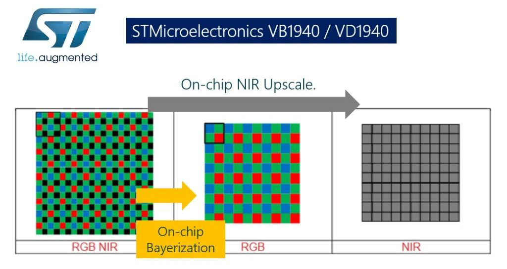
Figure 8. STMicroelectronics In-Cabin DMS / OMS with a 4×4 Pattern RGB-NIR and on-chip ISP Bayerization or NIR Upscale.
STMicroelectronics also displayed the VB56G4A, a 1.5MP Monochrome (NIR) sensor, with 2.61 µm pixel-pitch also Stacked Back-illuminated with Global shutter. According to STMicroelectronics, both the VB1940 / VD1940 and the VB56G4A sensors utilize Voltage-Domain Global Shutter where the photo-generated signal is stored after the charge-to-voltage conversion.
A Metal-Insulator-Metal (MIM) capacitor used for in pixel storage, is implemented in the CIS. Here, special precautions are taken into consideration to reduce Parasitic Light Sensitivity (PLS) of the MIM storage capacitor in the CIS to achieve efficient shuttering. According to STMicroelectronics, this helps reduce the sensor cost associated with implementing the Global Shutter storage in the stacked ISP.