Power Blog
Atom Probe Tomography of Silicon Carbide JFETs

Stephen Russell
Co-authored by: Ramya Cuduvally (affiliation: CCEM and Department of Materials Science and Engineering, McMaster University)
Brian Langelier (affiliation: CCEM and Department of Materials Science and Engineering, McMaster University)
Last year we demonstrated through a series of blogs the power of electrical characterisation to yield device characteristics far beyond what datasheets can offer.
Various techniques exist to analyze doping in semiconductors, such as:
- Scanning capacitance microscopy (SCM) which we regularly include in our power reports, this gives us relative dopant analysis over a large area.
- Scanning resistance profilometry (SRP) and secondary ion mass spectroscopy (SIMS) can give quantitative analysis but are size limited. Discerning absolute values of dopant well concentrations <1 µm in width is challenging.
- Atom probe tomography (APT) is a technique that is ideally suited to small area analysis, it allows for both three-dimensional imaging at the atomic scale as well as chemical composition analysis. It can give fascinating insights regarding the depth profile and mass spectrum of the ions present at the same time.
The power of APT
APT works by combining the principle of Field-Evaporation (FE) with Time-of-Flight Mass Spectrometry (TOF-MS). Knowing the sequence of arrival of the ions at the detector and their (x,y) co-ordinates, a simple geometric projection-based algorithm can be applied to finally obtain a 3D reconstruction of the specimen. APT can potentially provide an outstanding spatial resolution ranging between 0.25 – 1.25 nm depending on the material being analyzed.
The sensitivity of APT, as one can expect, is limited solely by the counting statistics and can be as good as 10 atomic ppm if a large enough volume is probed. APT is thus a powerful 3D elemental mapping technique that can potentially yield near atomic-scale resolution and close to single atom detection efficiency.
We already have a significant collection of analysis in our library of UnitedSiC’s 4th generation SiC JFETs: SiC power floorplan report, power essentials summary and process flow analysis can be found in our subscriptions. This product has also been the subject of a previous blog as well as part of the blog series on electrical characterisation of SiC products going beyond datasheet parameters. Now working with colleagues at the Canadian Centre for Electron Microscopy (CCEM) in McMaster University, Ontario, Canada we have taken this analysis even further.
The CCEM houses a wide range of state-of-the-art electron and ion microscopes – as well as a CAMECA Local-Electrode Atom Probe (LEAP) 4000X HR (Figure 1). This instrument facilitates the study of nanoscale properties and phenomena for a diverse range of materials including metals, alloys, semiconductors, ceramics, minerals and even biological materials.
Particularly, for the analysis of semiconductor devices, in addition to quantitative 3D mapping of elements and visualization of various layers/interfaces, APT data can reveal interesting details such as dopant segregation to defects, concentration profiles across nanoscale features and interfaces, localized composition etc. This information can, in turn, provide invaluable insights into the device performance/failure as well as its fabrication process.
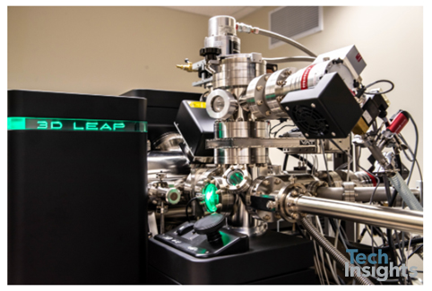
Figure 1: The CAMECA LEAP 4000X HR at CCEM
Target device – UnitedSiC 4th generation SiC JFET
The UnitedSiC UJ4C075018K4S is rated at 750 V with an on resistance (RDS.(ON)) of 18 mΩ. Our previous blog describes the benefits of this device (For further discussion see the full article)
These technological advances give a lower specific on resistance (RDS.ON(SP)) of 1.32 mΩ.cm2 in comparison to 3.03 mΩ.cm2 for its UnitedSiC 3rd generation counterpart. This is not only lower than UnitedSiC’s previous generation but lower than any 650 V SiC MOSFET we have observed to date. (Also note this is in fact a 750 V device).
The JFET array structure of the UJ4C075018K4S can be visualised in the scanning electron microscopy cross-section image in Figure 2. An SCM image in Figure 3 shows the relative doping and the p-type gate contact at the bottom of and along the trench sidewalls. It is this region (particularly at the trench bottom) that is of particular interest.
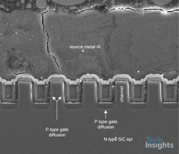
Figure 2: SEM cross-section image of UnitedSiC UJ4C075018K4S
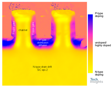
Figure 3: Scanning Capacitance Microscopy (SCM) image of UnitedSiC UJ4C075018K4S detailing relative dopant concentration
Historically p-type doping in SiC has been challenging. Aluminium (Al) is the best acceptor candidate, however Al implanted 4H-SiC is <10 % electrically activated with an anneal of 1400° C. It takes an anneal of 1600° C to approach 100% activation.
The challenges associated with p-type doping and associated issues such as lifetime killing defects from implantation and lattice distortions from high temperature anneals are a large contributing factor as to why we have yet to see commercially available bipolar power semiconductor devices such as IGBTs in SiC.
APT of the UJ4C075018K4S device
The magnitude of the surface electric field required to enable FE can be as high as a few tens of V/nm, which is nearly impossible to achieve in a laboratory set-up. To circumvent this, an APT specimen is essentially prepared in the form of a needle-shaped volume with an apex diameter of the order of 50-100 nm such that the application of a few kV can produce the desired magnitude of surface electric field. APT sample preparation is thus, a non-trivial process and requires dedicated instrumentation. Targeted lift-out and shaping of the region of interest (ROI) is achieved using a highly focused and energetic beam of ions (typically Ga or Xe), while imaging it using a scanning electron beam.
An SEM image of the SiC JFET APT specimen, which was sharpened using the dual beam Zeiss NVision 40 (Ga beam) is shown in Figure 4.
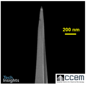
Figure 4: An SEM image of the Si JFET sample ready for APT analysis
The objectives of the current investigation were to quantify the p-type dopant in the channel of the SiC JFET and visualize its 3D distribution therein. Two successful APT experiments were conducted with 34 and 37 million ions collected, respectively. The p-type dopant was confirmed to be Al. After resolving the mass peak overlaps, the Al content in each specimen could be quantified within reasonable error and yielded an average value of 1e-19 atoms/cm3 (Table 1). Also indicated in the same table is the Si, C and Al content determined from each experiment.
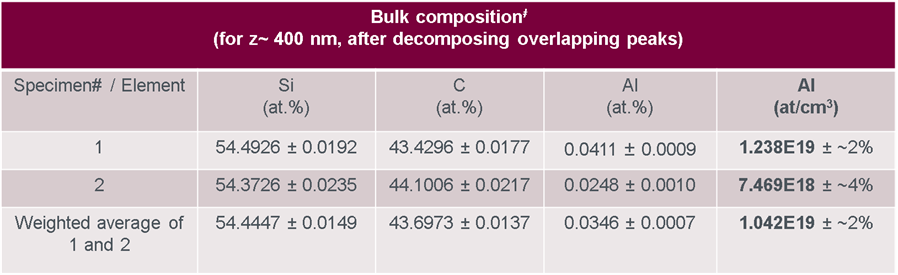
Table 1: Composition of the JFET gate region determined by APT
Interestingly, the APT reconstruction revealed an extremely inhomogeneous distribution of the Al inside the gate region indicative of its segregation to crystallographic defects in the SiC (Figure 5). These defects might be a result of the ion implantation process, with the number of Al atoms in each such cluster containing approximately 1000 Al atoms. As one might expect, such localized and random composition inhomogeneities within the device channel are undesirable since they could potentially increase the variability in the device performance and ultimately degrade the reliability.
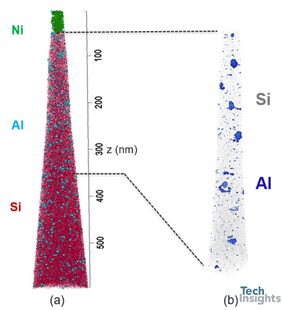
Figure 5: (a) The APT reconstruction of the analyzed volume obtained based on the SEM image shown in (b) Iso-concentration surfaces within the ROI having Al > 0.35 at. %, highlighting the Al-rich clusters inside the JFET gate region.
Summary
Having demonstrated through this work that APT can be used to gain highly localized information from semiconducting devices, in the future, we hope to extend our analysis to investigate the dopant distribution along the sidewalls, the quality of the SiC/SiO interface and the local composition variations within the Ni silicide gate.
References
- Atom Probe Tomography of Silicon Carbide JFETs (Part One) (TechInsights) 2022.
- Going Beyond Datasheets; Benchmarking and Testing the Performance of SiC FETs (Part One) ( TechInsights) 2021.
- B. Gault, A. Chiaramonti, O. Cojocaru-Mirédin, P. Stender, R. Dubosq, C. Freysoldt, S.K. Makineni, T. Li, M. Moody, J.M. Cairney, Atom probe tomography, Nat. Rev. Methods Prim. 1 (2021) 51.
- B. Gault, M.P. Moody, J.M. Cairney, S.P. Ringer, Atom Probe Microscopy and Materials Science, in: Springer Science & Business Media, 2012: pp. 299–311.
- W. Lefebvre-Ulrikson, F. Vurpillot, X. Sauvage, Atom probe tomography - Put Theory Into Practice, Academic Press, 2016.
- UnitedSiC Introduces New SiC FET Devices Based on Advanced Gen 4 Technology (UnitedSiC Website) 2020.
- UnitedSiC 750 V 18 mΩ SiC FET Power Floorplan Analysis (PFR-2101-804) TechInsights, 2021.
- UnitedSiC UJ4C075018K4S 750, 18 mΩ Gen. 4 SiC FET Power Essentials (PEF-2101-801) TechInsights, 2021.
- UnitedSiC UJ4C075018K4S 750 v 18 mΩ Gen. 4 SiC FET Process Flow Full (PFF-2103-802) TechInsights, 2021.
- UnitedSiC 4th Generation JFET Technology Demonstrates Record Breaking Performance, Where Next? (TechInsights) 2021.
- UJ4C075018K4S Datasheet (UnitedSiC Website) 2022.