Logic Analysis Blog
Apple M1 Ultra Advanced Packaging
Innovative packaging architecture using Apple's UltraFusion.
Richard Li

John Boyd
Packaging has become more sophisticated and a differentiator in the overall performance of advanced SoC chipsets. It can significantly impact form factor, helping to miniaturize designs in the multichip package and improve chip-chip RC delay. TechInsights’ packaging analysis products provide insight into advanced chipset packaging innovations.
Heterogenous integration (HI) continues as a critical driving force in developing and adopting advanced packaging technologies. During the last four months, our Packaging channel has issued reports on two milestone devices from leading manufacturers: The Apple M1 Ultra processor from the Mac Studio desktop computer and AMD’s Ryzen 7 5800X3D gaming processor featuring integrated 3D vertical cache (V-Cache). Both devices leverage TSMC’s advanced packaging offerings and offer compelling visions of a future advanced packaging landscape.
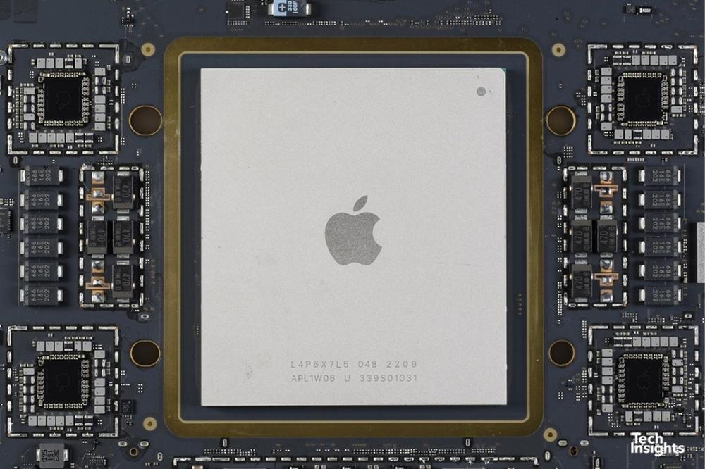
Figure 1. Apple M1 Ultra processor
The Apple M1 Ultra package drives the M1 Max system-on-chip (SoC) to its logical destination by using a silicon (Si) bridge die to connect two identical processors. The large unused region of high-density interconnect observed on the M1 Max processor enables the high-speed and high-bandwidth bridge. However, TSMC’s integrated fanout local silicon interconnect (InFO-L) technology is vital. The Si bridge ties the processors together and enables low resistance, low latency, and high bandwidth. The Ultra is the first example of a device utilizing InFO-L technology that TechInsights has documented.
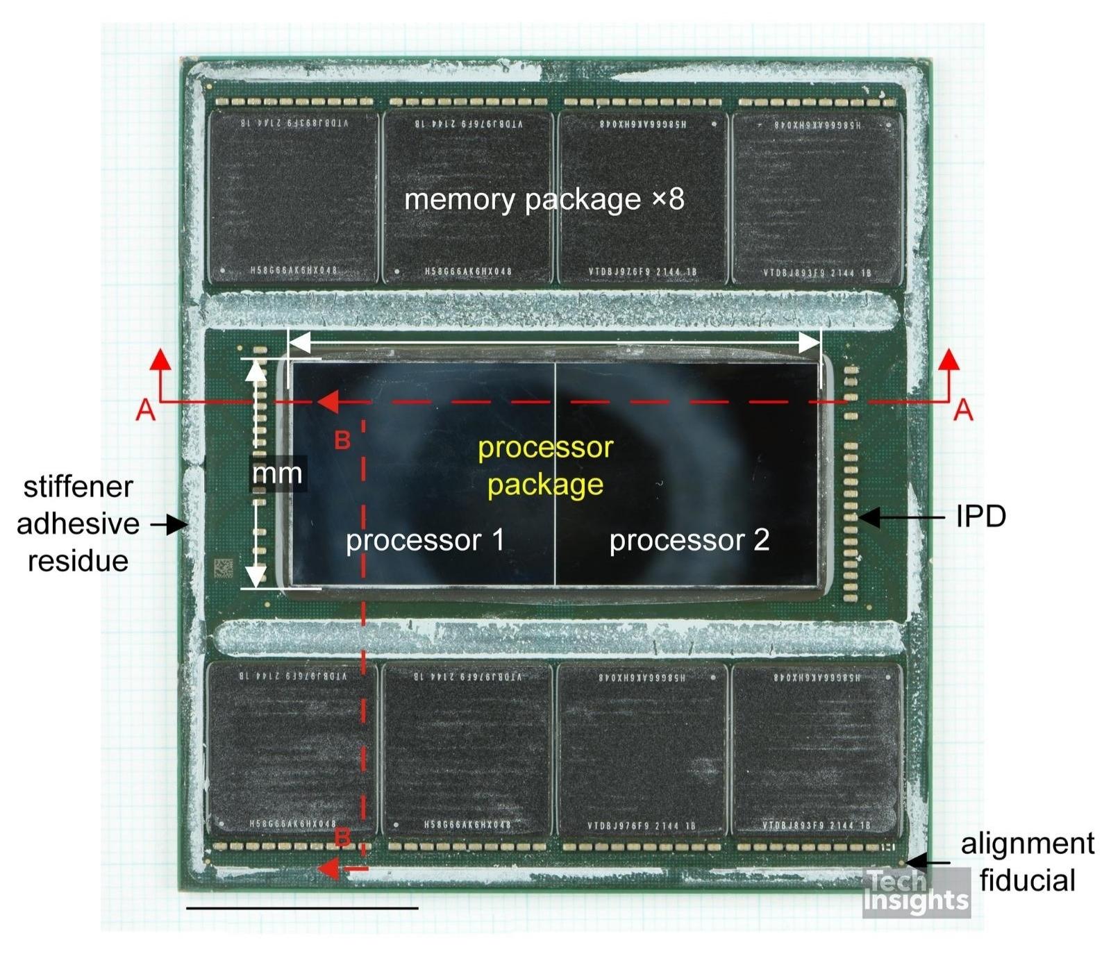
Figure 2. Apple M1 Ultra package (top view) after removal of heat spreader and stiffener
A single M1 Max processor is a large die at >400 mm2, but a significant portion is devoted to the high-density interconnect pads required to connect to the Si bridge. Apple pays that area and cost penalty for each M1 Max it produces, even for those chips that do not end up in an Ultra package. These extra costs come directly from adopting the local area silicon interconnect packaging strategy, so what benefits drive Apple towards this trade-off?
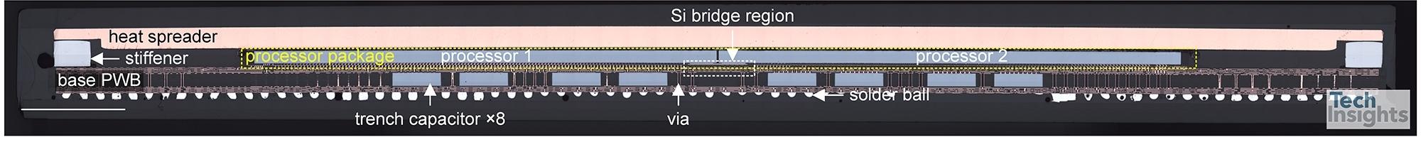
Figure 3. Apple M1 Ultra package (cross-sectional view)
The practicality and cost of producing a die almost twice as large as the M1 Max are undoubtedly one of them. Built on an advanced TSMC 5 nm node and pushing towards the maximum reticle limit, this hypothetical processor can also be expected to suffer higher proportional yield losses than the M1 Max. This perspective makes splitting the die and creating a product like the M1 Max processor attractive.
Beyond practicality, the decision to make two separate products (the Max and the Ultra) from a single SoC comes with a host of other design and operational benefits. A single part number will simplify supply chains and reduce overhead throughout the production cycle.
Designing a product like the M1 Ultra presents a problem without a solution at the die level. Instead, a packaging solution is required, which is precisely the route Apple has taken. That solution comes with costs and benefits, which all manufacturers must consider when deploying similar packaging technologies.
Want to know more? Subscribe to TechInsights Logic Advanced Packaging Channel to see the full report, or click here for trial access.