Apple Joins 3D-Fabric Portfolio with M1 Ultra?
On March 8, Apple held their “Peek Performance” event, introducing the all-new Mac Studio and Studio Display, a new iPad Air, the new iPhone SE, and two new shades of green for the iPhone 13 and iPhone 13 Pro.

Dick James
M1 Ultra Announcement
The iPhone and iPad models are evolutionary upgrades, but the Mac Studio desktop and Studio Display are new products. The Studio PC in particular attracted my attention, since its processor is a step up in Apple silicon capability. We have been anticipating an enhancement to the M1 series of chips to an “M2” series, but in the Studio we have the option of the M1 Max or the new “M1 Ultra”, apparently the last of the M1 line.
The “M1 Ultra is another game-changer for Apple silicon that once again will shock the PC industry. By connecting two M1 Max die with our UltraFusion packaging architecture, we’re able to scale Apple silicon to unprecedented new heights,” according to Johny Srouji, Apple’s SVP of Hardware Technologies.
So – “connecting two M1 Max die with our UltraFusion packaging architecture” – connecting two processor dies with what sounded like an interposer or a silicon bridge. In the presentation, Johny Srouji said “the UltraFusion architecture uses a silicon interposer that has twice the connection density of any technology available”.
The M1 Max is ~19.05 x 22.06 mm, or ~420.2 mm2, so even with die edge contacting die edge, a TSMC CoWoS-style interposer would be a minimum of 840 mm2, right at the reticle limit. And that’s a lot of silicon, (i.e. expense), so now that we have bridge technology such as Intel’s EMIB, that seems more likely.
Apple’s graphics seem to show that:
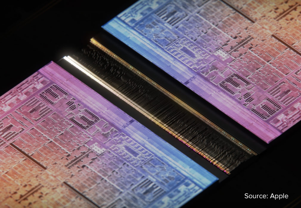
Figure 1. Source Apple.
Subscribe to TechInsights Blogs
Join our list to get the latest blog posts directly in your email.
Merging the two dies with the bridge:
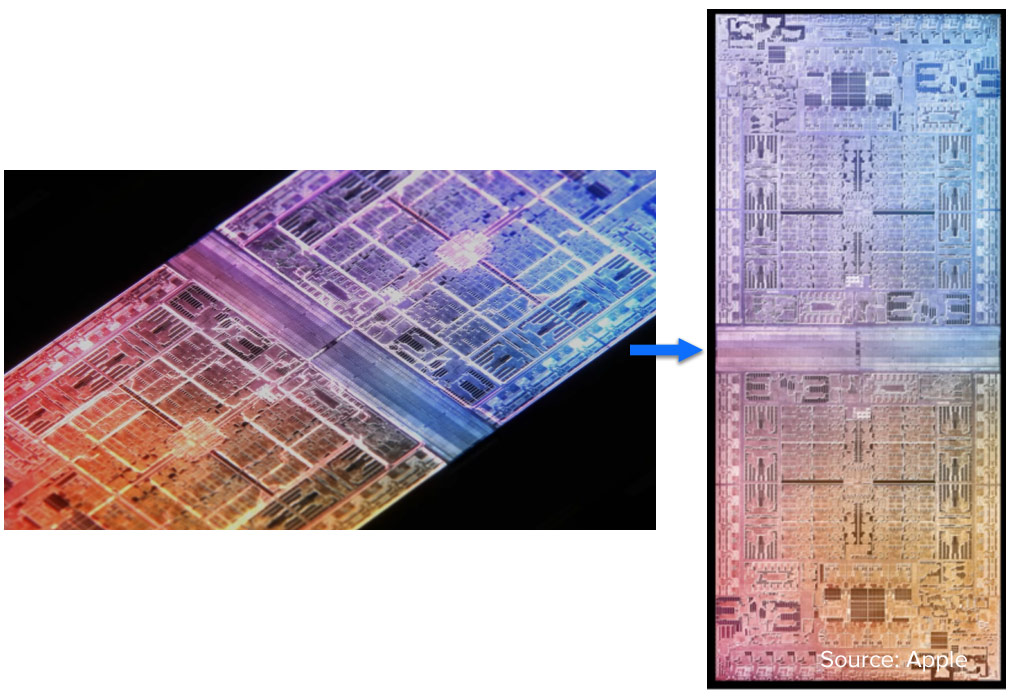
Figure 2. Two die photos with the bridge.
One of the surprises that came out of the talk was that the M1 Max was already designed with the interconnect circuitry on-chip. And when we looked, there it was at the bottom of the die:
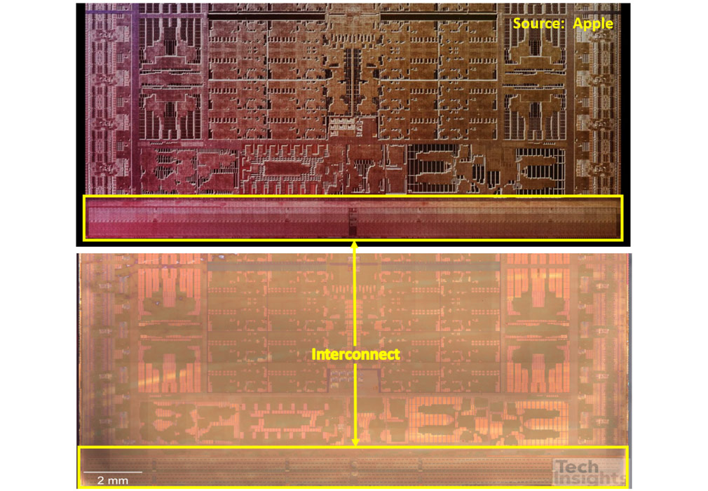
Figure 3. Apple M1 MAX APL1105 processor designed with the interconnect circuitry on-chip.
In our DFR-2111-801 floorplan analysis we had conservatively labeled that area as digital logic blocks; now we know their function. Looking closer:
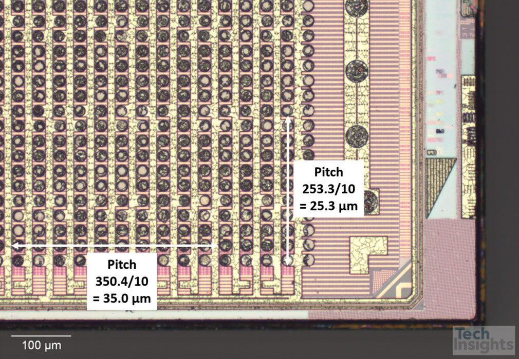
Figure 4. Apple M1 MAX APL1105 die photo.
Ensure you’re armed with the latest technical intelligence.
Sign up for a free trial today to see how the TechInsights Platform will help you.
Sample reports from this blog may be available with your free trial.
The bump pad pitch has been squeezed down to 25 µm.
TSMC has announced two versions of a silicon bridge technology, InFO_LSI and CoWoS-L.
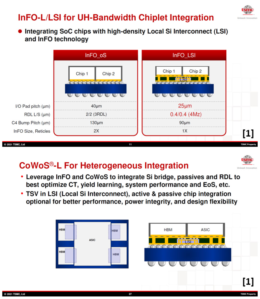
Figure 5. TSMC InFO_LSI and CoWoS-L.
To me they look the same:
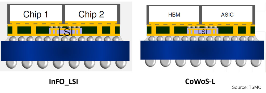
Figure 6. Silicon bridge technology comparison.
We don’t have any numbers for CoWoS-L, but the InFO_LSI bump pad pitch is specified at 25 µm, the same as we see in the interconnect area of the M1 Max. So knowing the tight relationship between Apple and TSMC, it is tempting to assume that their “UltraFusion packaging architecture” is at least a customized version of InFO_LSI/CoWoS-L.
The RDL (redistribution layer) line/space dimensions of InFO_LSI are 0.4/0.4 µm, which implies an I/O density of 1250/mm/layer. Given that the die edge on the interconnect side is over 18 mm long, that gives us over 20,000 potential I/Os, way more than the 10,000 quoted by Srouji. For comparison, Intel’s EMIB is 250/mm/layer or greater with the existing 55-µm bump pitch; and of course they will be working on increasing that density.
The combined SoC has 114 billion transistors, and doubling up the M1 Max makes it a part with a 20-core CPU, a 64-core GPU, and a 32-core Neural Engine. It can be built with up to 128GB of LPDDR5-6400 unified memory with a stated 800GB/s of memory bandwidth.
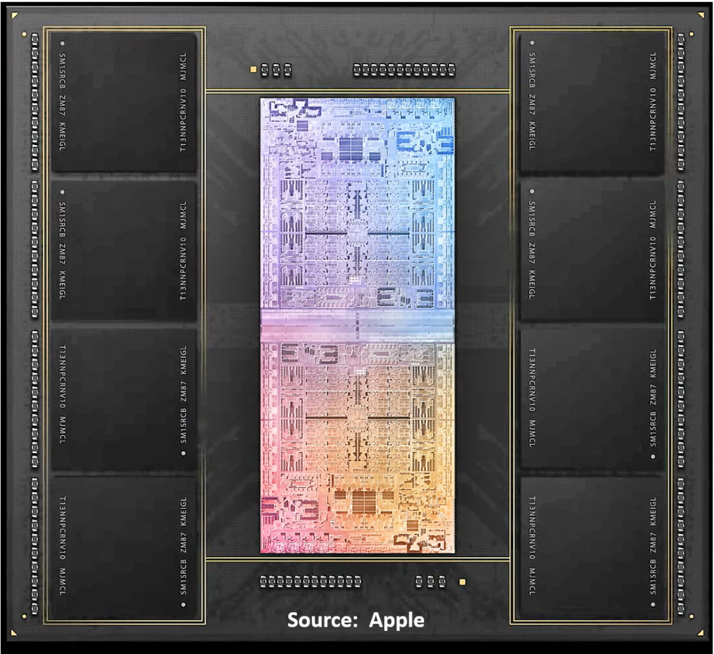
Figure 7. M1 Max.
The 10,000 signals is claimed to provide 2.5TB/s of low latency, inter-processor bandwidth between the two M1 Max chips. This allows the M1 Ultra to behave and be recognized by software as one chip, eliminating the need to rewrite code for the new structure. The macOS Monterey has been designed for Apple silicon, and will take advantage of M1 Ultra’s extra CPU, GPU, and memory capability.
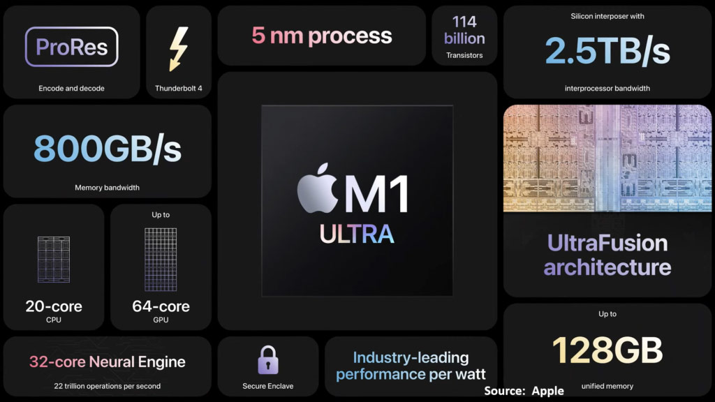
Figure 8. M1 Ultra.
All in all, an impressive announcement, and the Apple studio with the M1 Ultra will be available on March 18, so we do not have to wait for long to see what “UltraFusion” is.


