Apple AirTag Teardown
Access the world's largest database of consumer electronics and semiconductor reverse engineering
TechInsights has analyzed tracking devices for a few years now, from kid tracker wristwatches to the more recent tag-trackers like the Apple AirTag and the Samsung SmartTag+. That is to say - trackers have been on the market long before Apple released their AirTag last April.
Our interest in tag trackers is how much technology has evolved. We live in a world where a device the size of a US quarter-cent piece can have multiple antennas, radio ICs, a battery and continue to operate as a two-way radio, pinpointing objects within feet of accuracy for almost a full year.
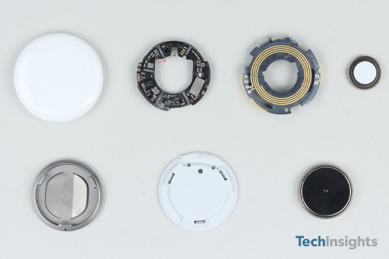
Figure 1. Apple AirTag Major Components
For example, ICs designed with smaller die process nodes. A die with a smaller process node means smaller transistor gate lengths, allowing for more transistors per die, reducing the IC’s power consumption because of the shorter transistor gate lengths.
The Apple AirTag has the Nordic nRF52832, whose die is built with a 90nm process node - an advancement over the 180nm process used in slightly older 2.4 GHz Noridc Transceiver ICs. The nRF52832 found in the AirTag is the WLCSP50 package which is 75% smaller than the larger 48-pin 6 mm x 6 mm QFN option. There may be multiple reasons for selecting the WLCSP50 instead of a QFN package, one of which could be as simple as requiring less PCB space to use the versatile Nordic chip.
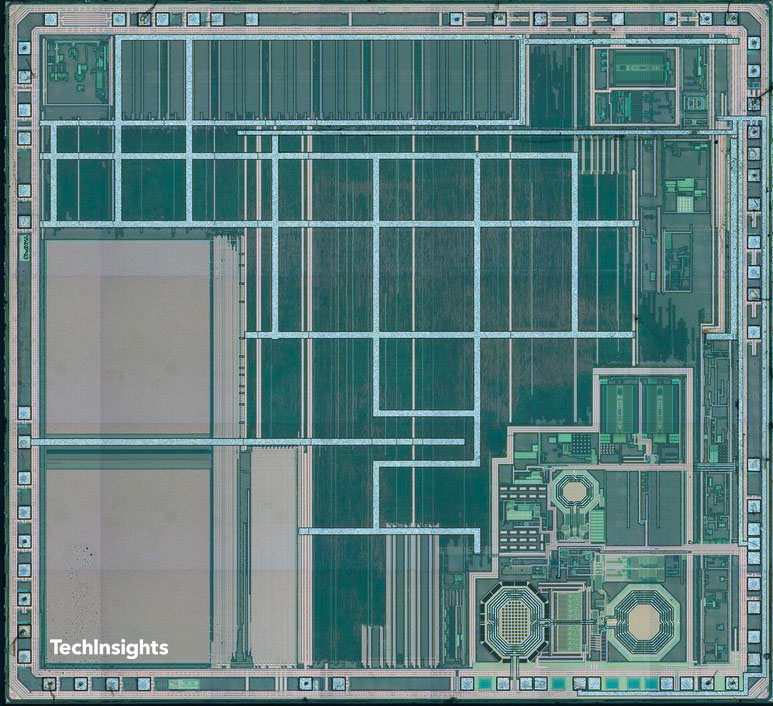
Figure 2. Nordic nRF52832 die photo
The nRF52832 Bluetooth SoC can support multiple radio types, including a 2.4 GHz proprietary radio if needed. The nRF52832 used in the Apple AirTag supports NFC tag, Bluetooth, and Bluetooth Mesh. It is the Bluetooth Mesh feature that enables the AirTag to connect to other Apple devices in the Apple Find My network.
Another example of IC package advancements is the ability to embed multiple components into a single IC package, with one of the benefits being the reduced PCB area for a circuit design. Multi-chip, multi-components package techniques are not new and continue to improve, incorporating more than just die. The Apple U1 UWB SIP (system-in-package) – has the Apple UWB Transceiver, an embedded crystal oscillator, a Sony RF Switch, and smaller discrete components inside a single package with a total package area of 20.58 mm2.
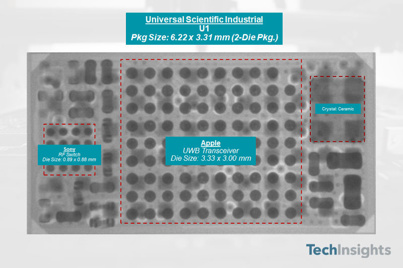
Figure 3. Apple U1 UWB SiP
For die size comparison to the nRF52832, the UWB transceiver die is fabbed on a TSMC’s 16nm process node, allowing for more transistors (and circuits) on a similar sized die like that in the nRF52832.
All in all, the radio ICs of the Apple AirTag take up less than 30 mm2, or 6%, of the entire available PCB area.
However, the performance of the AirTag, i.e., its success in staying connected to the Find My network, is not just in the radio ICs but also relies heavily on its antennas and antenna designs.
But the AirTag's small size does not allow for separate antenna parts as we see in other larger devices like mobile phones. Instead, the AirTag has a single frame with all three antennas designed on it.
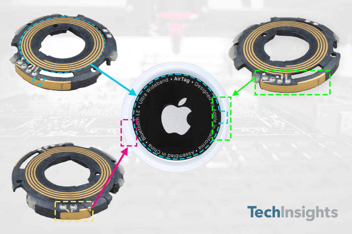
Figure 4. Apple AirTag Antenna Design
Apple also included a speaker in the AirTag, which 'chirps' for various scenarios. A Maxim Class-D audio amplifier also located on the PCB drives the speaker.
It is not just the AirTag’s function and design that are noteworthy. The AirTag retails for less than USD 30 and has an estimated manufacturing cost of USD 10 (not including software costs and R&D).
Trackers are not new, and Apple is not the first to offer such a product. Unfortunately, Apple is taking the brunt of the social recoil of how trackers may be used for invasive purposes. We are not sure if listing the technology inside these trackers helps put anyone’s mind at ease.
But for technology, there is no going back now, only forward. We believe new battery technologies like solid-state batteries, silicon batteries, and shrinking process nodes will only allow engineers in designing radio devices in even smaller packages.
Share with Colleagues
Related Analysis
WHOOP 4.0 Teardown
The new fitness wearable WHOOP 4.0 leverages a next-generation battery anode technology, which has the potential to raise the bar in the very competitive fitness and health monitoring market where major players such as FitBit, Xiaomi, and Apple lead.


