Contributed by: Arabinda Das
Today the semiconductor industry is a behemoth whose annual sales revenue crosses US $400 Billion. Over its 60 years of existence, this mature industry has experimented with various models like integrated device manufacturer (IDM), fabless, and foundry concepts, each of which adopted different intellectual property (IP) strategies.
In the early stages, between 1960 and 1970, designing an integrated circuit (IC) was a laborious task as it required specialized engineers who, without the help of electronic-design-automation (EDA) tools, had to manually create the circuits and layouts. This limited R&D to a select few manufacturers who could afford this costly process. At that time, the manufacturers had their patents centered around all aspects of their product.
In the early 1980s EDA tools started to appear on the market leading to a standardization of processes that enabled many more players to enter the manufacturing arena. This standardization helped split both the designing and manufacturing processes; it was now possible to design in one place and manufacture in another. This was a huge relief as manufacturing was becoming extremely expensive and required regular upgrades to the equipment and process. This split gave birth to various classifications such as IDM, fabless and foundry.
IDMs included the most resourceful organizations, like Texas Instruments, Intel, and IBM. They had a complete overview, from the design phase to the product. They also fabricated logic and memory devices which added a wide spectrum of patents to their portfolios. Figure 1 depicts a 1990 Texas Instruments (TI) 4MB CMOS DRAM from Techinsights’ library. This device employs a trench capacitor for data storage. Texas Instruments not only designed the DRAM, but also manufactured the device and packaged it all on their own site in USA. Today TI does not fabricate any more memory products or logic processors, but they still continue to monetize their vast intellectual property assets.
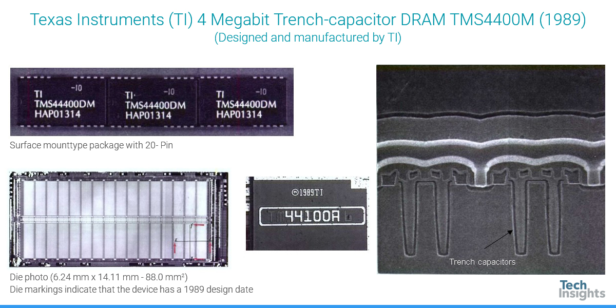
Figure 1: Early DRAM (1989-1990) from IDM Texas Instruments
The fabless model designed their own products but depended on foundries to manufacture them. Thus, fabless organizations concentrated exclusively on the functions and applications that their products could bring to the market, and they filed patents accordingly. Qualcomm was one of the pioneers to have embraced the fabless model which holds true even today. Figure 2 images are from Qualcomm - one created in the late nineties and another is one of their most recent devices; both were analyzed at Techinsights. The image on the left has die markings which indicate that the chip was manufactured by Intel. The image on the right was manufactured by Samsung.
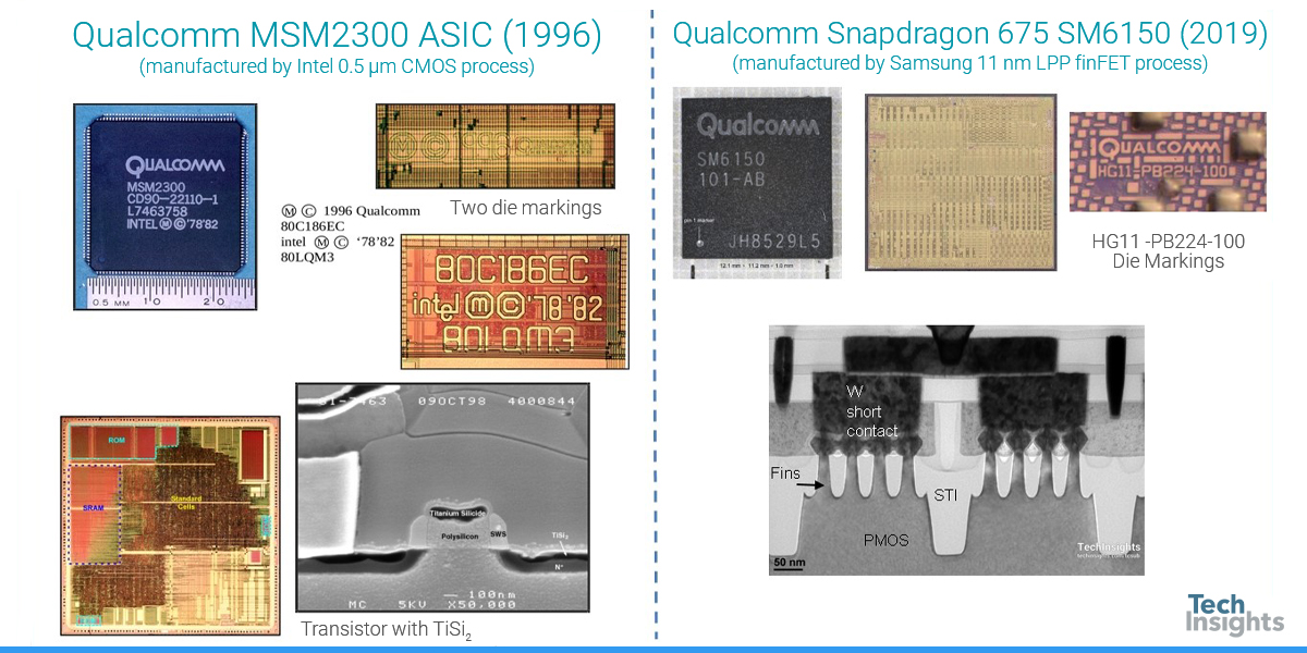
Figure 2: Two devices from fabless company Qualcomm from different times
The foundries were constantly confronted with manufacturing challenges like defect density, etch-selectivities, and filling of high aspect ratio structures, creating a need to constantly look for workarounds. Every major problem they solved resulted in a patent. For the next 10 years, the patent portfolios of the fabless and foundries remained quite distinctly apart. Over time, many IDMs dropped out of the semiconductor industry or adopted the fabless-foundry model; the challenge to maintain the entire semiconductor process required immense resources and savoir faire.
The turn of the millennium saw great progress in the semiconductor technology sector including the introduction of copper interconnects in 1997 by IBM, which was later adopted by all other logic manufactures. Copper interconnects brought new challenges such as chemical mechanical polishing of copper and tantalum-based barriers, via miss-alignments in Cu-Damascene structures and electromigration issues. All these issues were solved and generated an abundance of process patents from different manufactures. This period also experienced the apex of Moore’s law, which states that the number of transistors on a chip doubles every two years consequently making the cost of fabricating electronic devices much cheaper. During that period, a variety of chips were manufactured for a plethora of applications. These chips were mounted on different types of printed circuit boards and depending on the number of input/outputs their configurations could vary from wire bonding, to flip-chip, pin-grid arrays, surface mount technologies, and more. These package configurations and their processes were so different that they had to be taken up by a complete separate organization. The out-sourced-assembly-test (OSAT) was born in the late 1990s. The fabless-foundry model had already established its manufacturing sites in Asia while the design remained in the USA and Europe. The OSAT extended its spread even further to other countries in Asia. OSAT did a formidable job of testing the devices and packaging them and patenting the back-end process. One should not forget that a few IDMs, who kept a close eye on the entire process, contributed to many significant milestones in the packaging industry, such as the ball-grid array, and flip-chip copper pillar process. By the mid-2000s there were four distinct groups (IDM, foundries, fabless and OSAT) developing their own distinct IP.
The status quo of the chip ecosystem was disrupted by the introduction of the iPhone in 2007. Smartphones assembled in a small footprint have several components like display, touch screens, cameras, microphones, speakers, battery, sensors, antenna, Wi-Fi connectivity, memory, processors, storage and more not to mention all the different types of software which exist to facilitate daily operations. As smartphones developed, it became a dire necessity to innovate new compact packages, optimize the interconnect structures between disparate devices, and provide powerful computation capabilities to processors. Smartphones connected the general public to the internet and made the transfer of large amounts of data possible, ushering in the need for better data collection and manipulation. Data organizations required application specific processors which were not yet available in the market; this demand pressured companies to meet this need. As a result, the boundary line between the design-house, the foundry, and the software companies became quite blurred: Foundries began getting involved with design and packaging. Particularly, TSMC one of the leading foundries, expanded its portfolio in a variety of fields. Today, TSMC manufactures chips for various companies including Apple and has developed its own proprietary integrated fan-out (InFO) packaging technology, in which stacked DRAM dies are placed on top of an embedded processor that has redistribution lines on its molding compound. Figure 3 shows one of the latest packaging products by TSMC, which is used mainly for Apple processors.
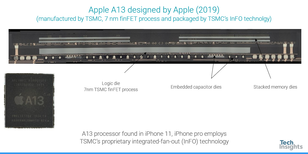
Figure 3: Integrated fan-out packaging from foundry TSMC
Similarly, data corporations like Microsoft, Apple, and Google started designing chips for their applications. This created a re-integration of the semiconductor process; the convergence of different organizations led to the creation of patents at the intersection of portfolios. In the future, there will be an even greater mix of patents from various groups with the emergence of technologies such as 5G.
Recently, I came across a detailed landscape report on 5G, presented by Ed White from Drewent [2]. One of the main takeaways was that the inventions of top 5G assignees (Samsung, Apple, Huawei, Qualcomm, Ericsson and Nokia) could be divided into thirty-seven technical categories. These six companies possess 41% of the 5G patents and none of them have any manufacturing capacity (Samsung being the exception). Nevertheless, they all have filed patents in all sorts of technical categories including healthcare, education, agriculture, automotive, multiple access schemes, antenna, and enhanced mobile broadband. This wide portfolio suggests that it is extremely difficult to categorize a company into a single box and assign it a unique specialization. Software companies, IDMs, foundries, and fabless are all filing patents over an entire, disparate spectrum.
The situation becomes even more complex considering that, in the era of 5G, new applications will emerge for some of the existing configuration. For example, one of the prominent technologies of 5G is Massive MIMO (Multiple-Input Multiple-Output) technology. MIMOs are configured to allow a wireless network to transmit and receive multiple data signals over a single radio channel. To make this possible, multiple antenna are needed on the same platform; as a result, future smartphones will have more sophisticated antenna structures. This concept has opened a novel package application called antenna in package (AIP) or antenna on package (AOP) which is a subset of embedded fan-out packaging. Embedded fan-out packaging was designed to incorporate actives and passives (such as the antenna, inductors and capacitors) in the package. Infineon was one of the pioneers of embedded fan-out packaging and their embedded-wafer-level-ball-grid-array (eWLB) was developed in 2008 and licensed to STATS ChipPAC, ASE and Amkor. The three OSAT companies made further developments to the original idea by offering solutions to integrate multiple actives and passives in the package, including antenna structures; this encouraged many other players to join the fan-out technology community. When Infineon built a precise motion detection device technology for the Google Pixel 4 smartphone in 2019, they did it without using their embedded fan-out technology. Instead, they incorporated the antenna in the printed circuit board, as deduced from the structural analyses performed at Techinsights [4,5]. This further reinforces the interdisciplinary mindsets that most modern tech giants are embracing. Today, there are at least ten companies that are directly involved in fan-out-wafer-level packaging [3], out of which eight are OSAT players.
In addition to categorical boundaries disappearing, the patent landscape is further complicated by the fact that intellectual property (IP) is constantly changing hands. According to IAM editor R. Lloyd the first quarter of 2020 saw the largest number of US patent deals and the largest amount of assets changing hands [6]. In fact, 2020 has seen the greatest movement of IP since the year 2010 when the tracking of the patent deals was monitored. IBM, LG and Nokia were some of the most prominent sellers while most buyers were non-practicing entities, however TSMC, Samsung and Sony were among the top five buyers. Clearly, the semiconductor industry has moved on from a time where a DRAM patent was only applicable to specific products. Today the technology is still fragmented into many specialized areas but at the same time the interfaces between different categories is more fluid than ever. The resulting patent landscape is challenging but also filled with opportunities for intellectual property practices. There is no single strategy for protecting one’s IP; one possible way forward is to accept the concept of Open-Innovation. The main idea of Open-Innovation is to integrate or accept ideas and technologies from an outside organization in order to enhance one’s own innovation [7]. This allows semiconductor companies to focus on their core strengths and rely on massive collaboration with other companies and/or research consortium in areas where they don’t have the required skills. Here’s hoping that the future of IP focuses on the emergence of creativity, which is so characteristic of the semiconductor industry. Meanwhile, Techinsights is continuing to track the advances in technology and keeping an eye on the changing landscape of patents.
TechInsights exists to support a fair marketplace where semiconductor and electronics intellectual property can be innovated and monetized. We are a world leading provider of advanced technology analysis and intellectual property services.
Our analysis quantifies the unknown to help you make informed decisions. We can determine what it will cost to bring advanced memory to market, we research potential market challenges to help you determine what your risks are, and we help define your de-risking strategy.
References:
[1] https://www.semiconductors.org/the-2020-sia-factbook-your-source-for-semiconductor-industry-data/
[2] Identifying opportunities in 5G landscape, by Ed White, IAM winter 2019
[3] https://semiengineering.com/fan-out-wars-begin/
[4] https://www.infineon.com/cms/en/about-infineon/press/press-releases/2019/INFPMM201910-003.html
[5] Infineon 6TR13C Package briefings 2019, Techinsights
[6] https://www.iam-media.com/non-practising-entities/new-data-points-bumper-first-quarter-of-patent-deal-making
[7] Everything You Need to Know About Open Innovation
Open Innovation and Intellectual Property Rights- The Two-edged Sword


